Play all audios:
ABSTRACT A surface plasmon (SP) is a fundamental excitation state that exists in metal nanostructures. Over the past several years, the performance of optoelectronic devices has been
improved greatly via the SP enhancement effect. In our previous work, the responsivity of GaN ultraviolet detectors was increased by over 30 times when using Ag nanoparticles. However, the
physics of the SP enhancement effect has not been established definitely because of the lack of experimental evidence. To reveal the physical origin of this enhancement, Kelvin probe force
microscopy (KPFM) was used to observe the SP-induced surface potential reduction in the vicinity of Ag nanoparticles on a GaN epilayer. Under ultraviolet illumination, the localized field
enhancement induced by the SP forces the photogenerated electrons to drift close to the Ag nanoparticles, leading to a reduction of the surface potential around the Ag nanoparticles on the
GaN epilayer. For an isolated Ag nanoparticle with a diameter of ~200 nm, the distribution of the SP localized field is located within 60 nm of the boundary of the Ag nanoparticle. For a
dimer of Ag nanoparticles, the localized field enhancement between the nanoparticles was the strongest. The results presented here provide direct experimental proof of the localized field
enhancement. These results not only explain the high performance of GaN detectors observed with the use of Ag nanoparticles but also reveal the physical mechanism of SP enhancement in
optoelectronic devices, which will help us further understand and improve the performance of SP-based optoelectronic devices in the future. SIMILAR CONTENT BEING VIEWED BY OTHERS NANOSCALE
LIGHT FIELD IMAGING WITH GRAPHENE Article Open access 29 June 2022 DUAL-PULSE PHOTOACTIVATED ATOMIC FORCE MICROSCOPY Article Open access 24 August 2021 SPONTANEOUS AND STIMULATED
ELECTRON–PHOTON INTERACTIONS IN NANOSCALE PLASMONIC NEAR FIELDS Article Open access 15 April 2021 INTRODUCTION A surface plasmon (SP) is an optical phenomen on that involves collective
oscillations of charges that are confined to nanostructured metal systems1. One of the most fundamental properties of a SP is the localization of the electromagnetic field. By nature, the SP
eigenmodes of small nanoplasmonic systems are localized and nonpropagating. SP has delivered a number of important applications: ultrasensing2, scanning near-field optical microscopy3,
thermally assisted magnetic recording4, biomedical tests5 and SP-assisted thermal cancer treatment6. Surface plasmon amplification by stimulated emission of radiation (SPASER), a
nanoplasmonic counterpart of the laser, was proposed in theory by Bergman and Stockman and has been realized in experiments7, 8, 9. Moreover, SP has offered new opportunities to improve the
performance of semiconductor optoelectronic devices. Metallic nanostructures have been used to modify the local density of optical states to control light emission, enhance photoluminescence
and reduce the quantum-confined Stark effect in light emitting diodes (LEDs)10, 11, 12. Plasmonic metallic nanoparticles have also been integrated into photovoltaic devices to increase the
solar cell absorption via light-trapping effects and enhance the short-circuit photocurrent density13, 14, 15, 16, 17. In our previous work, we realized high-performance GaN detectors by
fabricating Ag nanoparticles on the surface of the GaN epilayer; the responsivity of the GaN detectors increased by over 30 times. The localized SP effect was considered the reason for this
enhancement18, 19, as elaborated in our previous report. Here, the ‘enhancement’ refers to an increase in responsivity of the treated GaN detector and not to an optical electric field
intensity increase due to local plasmonic resonance. However, the direct evidence for this hypothesis is still lacking, and the physical origin behind the SP enhancing the performance of
semiconductor photoelectric devices remains to be clarified. Hence, a feasible method is urgently required to explain the SP enhancement. Here we propose a method to detect the SP-induced
localized field variation of Ag nanoparticles on GaN epilayer using Kelvin probe force microscopy (KPFM). As an electrical analog of atomic force microscopy (AFM), KPFM is typically used to
observe the surface potential20, 21, 22, 23. The electrical properties, such as the polarity24, 25, doping type26, 27, homogeneity28 and charge density29 of the sample, have all been
identified using KPFM. Based on the theory that the localized field enhancement by SP will adjust the dispersion of the electrons in the GaN epilayer, KPFM was adopted here to verify the
existence of the plasmon-enhanced field. Under ultraviolet (UV) illumination, the surface potential around a Ag nanoparticle on the GaN epilayer was reduced, thereby providing direct
evidence for the SP-induced localized field enhancement. Our direct observation of the SP effect can open ample avenues to integrate SP into future optoelectronic devices. MATERIALS AND
METHODS The undoped GaN epilayer was grown on a (0001) sapphire substrate using metal-organic chemical vapor deposition at 1050 °C. Details of the GaN epilayer growth can be found in
previous work18. The Ag nanoparticle was fabricated by electron beam evaporation at a pressure of ~5.4 × 10⁻⁶ mbar. The evaporation rate was ~0.1 nm s−1. Next, the sample was annealed at 800
°C for 5 min to form Ag nanoparticles. The Bruker multimode-8 AFM tapping mode was used to characterize the morphology, and the KPFM mode was used to determine the surface potential of the
Ag nanoparticles on the GaN epilayer. The tip was a Pt/Ir-coated tip, and the lift height for the interleaved mode was set to be 100 nm. When we used the KPFM to measure the surface
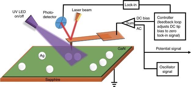
potential of the Ag nanoparticles on the GaN epilayer, the laser beam illuminating the tip was reflected on the photodetector. The alternating current (AC) bias was used as an oscillator
signal to allow the tip to oscillate at its resonance frequency. The direct current (DC) bias was used to adjust the amplitude of the oscillation to zero as the lock-in signal. In addition,
an external UV source was used to enable the measurement of the change of the surface potential without and with UV illumination. Time-domain and frequency-domain finite-element methods were
used to simulate the distribution of electric field of a Ag nanoparticle under UV illumination. RESULTS AND DISCUSSION A schematic principle of using KPFM to detect the surface potential is
given in Figure 1. In KPFM mode, the tip is driven by the applied AC at the same frequency as the resonance frequency (_ω_) of the tip. As the tip scans the sample, it also vibrates. When
KPFM is used to measure the surface potential of the Ag nanoparticles on a GaN epilayer, the tip lowers such that it is close to the surface of the sample. At this stage, the contact
potential (_V_CPD) appears and modulates the vibration of the tip. Moreover, there is a direct voltage biased on the tip (_V_bias). The values of _V_CPD and _V_bias are used to determine
Δ_V_DC according to Equation (1). Thus, the active forces on the tip originate from both the alternating voltage (_V_ACsin(_ωt_)) and the directive voltage (Δ_V_DC)30, 31, 32. The equation
for the force is given as follows: In succession, Equation (3) can be deduced, where the coefficient of Sin(_ωt_) is the amplitude of the vibration of the tip. The KPFM feedback loop is used
to adjust the _V_bias to be equal to _V_CPD and achieve Δ_V_DC=0. Thus, when the amplitude is zero and then the value of _V_CPD is obtained. In our experiment, the value of _V_CPD is the
difference between the surface potential of the sample and the potential of the tip, as given by Equation (4): The relationship among the _V_CPD, the work functions of the sample
(_φ_Sampl_e_) and the tip (_φ_Tip) can be written as31, 32, According to this relationship, a smaller _V_CPD corresponds to a higher _φ_Sample. Thus, under UV illumination, the decrease of
the surface potential around the Ag nanoparticle corresponds to an increase of the surface work function. The morphology of the Ag nanoparticles on the GaN epilayer was measured using AFM in
tapping mode. The semi-spherical isolated Ag nanoparticles and dimer Ag nanoparticles are located randomly on the GaN epilayer, as shown in Supplementary Figs. S1 and S2. Figure 2a shows
the typical morphology of the Ag nanoparticles on the GaN surface. The red and green lines are marked crossing the isolated Ag nanoparticle to describe the characteristics of the Ag
nanoparticles clearly. The diameters of this Ag nanoparticle are 205 and 220 nm, corresponding to the red and green lines, respectively. The height of the Ag nanoparticle is ~80 nm,
according to the section profiles of height given in Figure 2b. For the dimer of Ag nanoparticles, the black line crosses the two adjacent nanoparticles, as shown in Figure 2a. For the left
and right nanoparticles of the dimer, the diameters are 278 and 229 nm, respectively, with corresponding heights of 70 and 60 nm, respectively. The surface potential of a Ag nanoparticle on
GaN was obtained by AFM using KPFM mode. Figure 2c and 2d, shows the measured surface potential in the dark and under UV illumination, respectively. Figure 2c indicates that under dark
conditions, the surface potential of the isolated Ag nanoparticle was slightly higher than that of GaN. The section profiles of the surface potential along the same lines as the red and
green lines are given in Figure 2e. In the dark, the surface potential of isolated Ag nanoparticle was ~3.415 V, which was higher than that of the GaN epilayer (3.400 V). The diameters of
higher surface potential region were ~204 and 220 nm along the red and green lines, respectively, which were nearly equal to the size of the Ag nanoparticle. This result indicates that the
surface potential in the dark was the intrinsic surface potential of the sample. Under UV illumination, the section profiles of the surface potential along the red and green line directions
are shown in Figure 2f. The surface potential of the GaN epilayer next to the Ag nanoparticle (3.165 V) was lower than that of the GaN epilayer far from the nanoparticle (3.185 V). The
diameter of the lower surface potential region was ~315 and 345 nm along the red and green lines, respectively. After subtracting the size of the Ag nanoparticle, the length of the surface
potential reduction region was ~55 and 63 nm along the red and green directions, respectively. A similar phenomenon was observed in the two adjacent Ag nanoparticles. For the dimer Ag
nanoparticles on the GaN epilayer, three positions were marked with numbers 1–3 on the black line, as shown in Figure 2a. Position 1 was located far from the Ag nanoparticle, position 2 was
in the vicinity of the Ag nanoparticle and position 3 was between the Ag nanoparticles of the dimer. In the dark, the surface potentials of positions 1, 2 and 3 are shown in Figure 2g; these
surface potentials were found to be the same (3.400 V) as that of the isolated Ag nanoparticle in dark (Figure 2e). Under UV illumination, the surface potential decreased from 3.400 V to
3.200 V, 3.170 V and 3.150 V for positions 1, 2 and 3, respectively, as shown in Figure 2h. The light intensity was uniform at the three positions; thus, the dependence of the effects of
photoillumination on the light intensity was not considered here. The reduction of the surface potential under UV illumination was observed for most of the Ag nanoparticles on the GaN
epilayer, as shown in Supplementary Fig. S1. As observed in the experiments, the distribution of the surface potential reduction at the GaN epilayer around a Ag nanoparticle was not uniform.
For an isolated Ag nanoparticle, the closer it is to the boundary of Ag nanoparticle, the lower the surface potential is. For the dimer Ag nanoparticles, the surface potential (_P_) for
positions 1–3 followed the sequence of _P_1>_P_2>_P_3. The contact between the Ag nanoparticles and the GaN surface should be a Schottky contact. However, the UV light cannot penetrate
the Ag nanoparticle to generate a photocurrent; thus, no Schottky current was observed here. Even if there is a Schottky current of electrons from metal to semiconductor, it is normal to
the surface of GaN and thus will not have an influence on the lateral decrease of the surface potential of GaN. According to the principle of KPFM, the surface potential is related to the
work function of the sample; thus, the band structure was analyzed schematically. The Schottky contact between the metal (Ag) and n-type GaN will lead to the pinning of the GaN conduction
band (CB) to a constant level at the surface, resulting in the bending downward of the CB in the bulk. However, the energy band we show here is not underneath the Ag/GaN contact; rather, it
is the energy band of the GaN in the vicinity of the GaN/Ag Schottky contact interface and the bulk GaN. Thus, the effect of the Ag/GaN Schottky contact on the surface potential can be
ignored. Here we take the typical dimer Ag nanoparticles as an example. In the dark, the surface potential at positions 1–3 has the same value of ~3.400 V. Under UV illumination, all of the
surface potentials at the three positions decreased. For position 1, which was far from the boundary of the Ag nanoparticle, the decrease of the surface potential originated from the surface
state of the GaN epilayer. There are empty donor surface states in the GaN epilayer that lead to the downward bending (_qV_D) at the surface of the GaN epilayer33, 34, as shown in Figure
3a. Under UV illuminates, the photogenerated electrons move to the surface states until the surface states become occupied with electrons and the band bending recovers to the flat band
condition (as shown in Figure 3b). As a result, the surface work function increased and the surface potential decreased from 3.4 to 3.2 V at position 1. At position 2, in the vicinity of a
Ag nanoparticle, the surface potential of GaN decreased from 3.400 V before UV illumination to 3.170 V and after UV illumination; that is, in addition to the electrons filling the surface
states, more electrons accumulated at position 2. These excess electrons caused the band to bend upward with the value ~30 mV, as shown in Figure 3c. At position 3, more electrons were
accumulated than at position 2. The surface work function increased further, and the surface potential decreased further, as observed in Figure 2d. The surface potential of GaN decreased
from 3.400 to 3.150 V. The band bent upward with the value ~50 mV. The only possible reason for the ultra-accumulation of electrons at positions 2 and 3 is the SP-induced localized field
enhancement by Ag nanoparticles. Under UV illumination, the SP effect results in localized field enhancement. Next, the plasmon-enhanced field drives the accumulation of photogenerated
electrons at the positions of the GaN epilayer in the vicinity of the Ag nanoparticles, leading to the increase of the surface work function, the upward bending of the energy band and, thus,
the reduction of the surface potential of the GaN epilayer. For the dimer Ag nanoparticles, because of the interaction between the particles, the electric field at the gap is higher than
that of at other positions. It can also be understood as follows: the electric fields generated by the two nanoparticles will be overlapped at the gap between the nanoparticles, resulting in
a higher electric field at position 3. More electrons are accumulated at this position, resulting in a higher surface work function and lower surface potential. Supplementary Fig. S1 also
shows that the decrease of the surface potential depends on the size of the Ag nanoparticles. Under UV illumination, obvious surface potential reduction was observed in the vicinity of the
Ag nanoparticles with sizes in the range of 140–280 nm (according to the statistical analysis of Supplementary Information S3), which again proved that the reduction of the surface potential
around a Ag nanoparticle originates from the SP-localized field enhancement. To further understand the analysis above, the surface spatial distributions of the electric field for Ag
nanoparticles on GaN was also simulated using time-domain and frequency-domain finite-element methods. We simulated the isolated and dimer Ag nanoparticles with diameter of 200 nm with the
gap of 30 nm. The incident wavelength was _λ_=350 nm. Figure 4a and 4b, shows the electric field distribution of semi-spherical Ag nanoparticles on the GaN epilayer. Under UV illumination,
localized field enhancement was observed to be generated in both isolated and dimer Ag nanoparticles. For the dimer Ag nanoparticles, the interparticle coupling interaction between the
particles causes the electric field to be the highest. Thus, our observation verifies that the cause of the enhanced responsivity of the GaN UV detector via Ag nanoparticles was due to the
localized field enhancement effect by SP. Theoretically, the enhancement factor depends strongly on the size and the surrounding dielectric environment of the particles. Based on SP theory,
if the nanoparticle sizes are less than 20 nm, then most of the energy of the SP collective modes is transferred to electronic transitions to induce hot carriers, whose distribution is quite
limited in a narrow phase space around the Fermi level. However, if the nanoparticle sizes are >20 nm, then most of the SPs’ energy is radiative, and photons are emitted35. In such a
case, the SP field can interact directly with the interband electronic transitions in dielectric materials when Ag nanoparticles are attached to the GaN surface. The interaction can be
dependent on the plasmon’s polarization and result in localized field enhancement. To understand the observed experimental results, we theoretically calculated the enhancement in the
polarizability for a spheroid with a>_b_, where _a_ and _b_ are semi-major and semi-minor axes of the spheroid, respectively. As shown in Figure 4, our FDTD simulation, using the Comsol
program, utilizes a numerical method to solve Maxwell equations. These simulations can provide the electric field distribution formed by the Ag nanoparticles but fail to provide us with the
physical insight that is required to understand the response of the metal particles to light. For the size of the nanogeometry considered in our experiment, a full analytical solution is
difficult to achieve. Nevertheless, for nanogeometries of sizes ~150 nm or higher, previous authors36 developed an analytical solution for the polarizability for a sphere and spheroid that
are in complete agreement with the experimental results. These simple and elegant solutions can be derived by an expansion of the first TM mode of Mie’s formulation. The retardation effect
is explicitly considered. We implement the analytical expression developed in Ref. 36 that also accounts for the effect that arises due to a finite speed of light for a spheroid with an
eccentricity, In Figure 5a, we plot the polarizability as function of energy for different sizes of nanospheroids with a vacuum dielectric environment. The polarizability is enhanced at ∼
3.400 eV, indicating that surface plasmons are excited on the metal surface and thus contribute to the enhancement of the responsivity obtained in our previous experiment18. It is useful to
analytically estimate the enhancement in response occurring around the GaN bandgap energy for smaller-sized nanoparticles by using the quasi-static approximation. This approximation works
well for small-sized nanoparticles and provides an estimate for larger-size nanoparticles if the dielectric environment is less dispersive (_ɛ_ is close to 1)37. The interaction between the
plasmon field and the electronic system in the bulk can be described by an interaction Hamiltonian38, where _b__c_(_b__v_) is the electron annihilation operator in conduction (valence) band
and _c__q_ is the plasmon annihilation operator. is the Rabi frequency for the interaction between plasmon of wave vector _q_ and the direct electronic transition with wave vector _k_ and is
given by where _e_ is the electronic charge, ψ_c_ (ψ_v_) is the conduction (valence) band wave function, _E_ is the plasmon field at the dielectric materials and R is the dipole radius
vector. Equation (7) shows that the plasmon field interacts directly with the electronic transition in the bulk. In nanoparticles of size where surface scattering of electrons contributes
significantly in plasmonic loss, a single quantum of plasmon decays in to a ‘hot’ electron–hole pair due to initial and final momentum difference of electron is contributed by the size
effect. However, for larger-sized nanoparticles, such an effect is strongly suppressed. The hot spot around the nanoparticles on the surface can generate a strong electric field, which can
induce a transition in GaN. The electronic transition probability per unit time induced by the plasmon field can be calculated using Fermi’s golden rule and is given by, where _P_cv is the
momentum matrix element in GaN and _m_ is the free electron mass. The delta function in Equation (8) ensures the momentum conservation without phonons. It can be easily shown that Assuming
that the fields do not penetrate and reach the substrate, the static plasmon field established on the surface of nanoparticle can be approximated by the quasi-static approximation as , where
_ɛ__d_ and _ɛ_(_ω_) are the dielectric for the medium and the metal, respectively, and _E__o_(_ω_) is the electric field of incoming photons. The dominant transition occurs at approximately
the gamma point of the Brillouin zone of GaN, the momentum matrix element for which is 8.85 × 10⁻²⁰ in cgs units39. A relevant quantity is a Poynting vector, _S_P, which describes the power
flow across an arbitrary cross-sectional area and is given by . In Figure 5b, we show the absorption per unit time using a plasmon field on the dielectric surface. The absorption rate is
proportional to the responsivity (that is, the absorption rate is also equivalent to the photocurrent). The calculation shows that because of the localized field enhancement effect by SP,
the enhancement can be up to 35 times with nanoparticles relative to the photocurrent of the device without nanoparticles. The photocurrent enhancement of a single nanoparticle is equivalent
to the average surface current per unit area of the aggregate nanoparticles. Note that the validity of the quasi-static approximation is limited to a regime in which the dipole radius
vector of the electro-mechanical oscillations (plasmon oscillation) that is covered in one optical cycle is comparable to the size of the nanoparticle (negligible retardation effect).
CONCLUSIONS Here we observed a reduction in the surface potential in the vicinity of Ag nanoparticles by using KPFM. Under UV illumination, for an isolated Ag nanoparticle of 200 nm in
diameter, the surface potential reduction region was within ~60 nm of the boundary of the Ag nanoparticle. For a dimer of Ag nanoparticles, the lowest surface potential was observed into the
gap between the Ag nanoparticles. We verified the SP-induced localized field enhancement by Ag nanoparticles on the GaN epilayer by using the undamaged method of KPFM. Based on the measured
SP effect, the physical mechanism for the enhanced UV responsivity of GaN detectors using Ag nanoparticles was also discussed theoretically. The results presented here not only provide
direct experimental proof to verify the localized field enhancement and allowed us to understand the SP effect further but may also accelerate the deployment of semiconductor optoelectronics
devices using SP enhancement. REFERENCES * Hutter E, Fendler JH . Exploitation of localized surface plasmon resonance. _Adv Mater_ 2004; 16: 1685–1706. Article Google Scholar * Anker JN,
Hall WP, Lyandres O, Shah NC, Zhao J _et al_. Biosensing with plasmonic nanosensors. _Nat Mater_ 2008; 7: 442–453. Article ADS Google Scholar * Mrejen M . Near-field imaging probes
electromagnetic waves. _Laser Focus World_ 2007; 43: 28–32. Google Scholar * Challener WA, Peng CB, Itagi AV, Karns D, Peng W _et al_. Heat-assisted magnetic recording by a near-field
transducer with efficient optical energy transfer. _Nat Photon_ 2009; 3: 220–224. Article ADS Google Scholar * Nagatani N, Tanaka R, Yuhi T, Endo T, Kerman K _et al_. Gold
nanoparticle-based novel enhancement method for the development of highly sensitive immunochromatographic test strips. _Sci Technol Adv Mater_ 2006; 7: 270–275. Article Google Scholar *
Gandra N, Portz C, Nergiz SZ, Fales A, Vo-Dinh T _et al_. Inherently stealthy and highly tumor-selective gold nanoraspberries for photothermal cancer therapy. _Sci Rep_ 2015; 5: 10311.
Article ADS Google Scholar * Bergman DJ, Stockman MI . Surface plasmon amplification by stimulated emission of radiation: quantum generation of coherent surface plasmons in nanosystems.
_Phys Rev Lett_ 2003; 90: 027402. Article ADS Google Scholar * Noginov MA, Zhu G, Belgrave AM, Bakker R, Shalaev VM _et al_. Demonstration of a spaser-based nanolaser. _Nature_ 2009; 460:
1110–1112. Article ADS Google Scholar * Apalkov V, Stockman MI . Proposed graphene nanospaser. _Light Sci Appl_ 2014; 3: e191. Article ADS Google Scholar * Su CY, Lin CH, Shih PY,
Hsieh C, Yao YF _et al_. Coupling behaviors of surface plasmon polariton and localized surface plasmon with an InGaN/GaN quantum well. _Plasmonics_ 2016; 11: 931–939. Article Google Scholar
* Cho CY, Park SJ . Enhanced optical output and reduction of the quantum-confined Stark effect in surface plasmon-enhanced green light-emitting diodes with gold nanoparticles. _Opt
Express_ 2016; 24: 7488–7494. Article ADS Google Scholar * Lozano G, Rodriguez SRK, Verschuuren MA, Rivas JG . Metallic nanostructures for efficient LED lighting. _Light Sci Appl_ 2016;
5: e16080. Article Google Scholar * Pryce IM, Koleske DD, Fischer AJ, Atwater HA . Plasmonic nanoparticle enhanced photocurrent in GaN/InGaN/GaN quantum well solar cells. _Appl Phys Lett_
2010; 96: 153501. Article ADS Google Scholar * Atwater HA, Polman A . Plasmonics for improved photovoltaic devices. _Nat Mater_ 2010; 9: 205–213. Article ADS Google Scholar * Su YH, Ke
YF, Cai SL, Yao QY . Surface plasmon resonance of layer-by-layer gold nanoparticles induced photoelectric current in environmentally-friendly plasmon-sensitized solar cell. _Light Sci Appl_
2012; 1: e14. Article Google Scholar * Chen X, Jia BH, Zhang YN, Gu M . Exceeding the limit of plasmonic light trapping in textured screen-printed solar cells using Al nanoparticles and
wrinkle-like graphene sheets. _Light Sci Appl_ 2013; 2: e92. Article ADS Google Scholar * Lu JF, Xu CX, Dai J, Li JT, Wang YY _et al_. Improved UV photoresponse of ZnO nanorod arrays by
resonant coupling with surface plasmons of Al nanoparticles. _Nanoscale_ 2015; 7: 3396–3403. Article ADS Google Scholar * Li DB, Sun XJ, Song H, Li ZM, Chen YR _et al_. Realization of a
high-performance GaN UV detector by nanoplasmonic enhancement. _Adv Mater_ 2012; 24: 845–849. Article Google Scholar * Fan XF, Zheng WT, Singh DJ . Light scattering and surface plasmons on
small spherical particles. _Light Sci Appl_ 2014; 3: e179. Article ADS Google Scholar * Yan F, Chen GN, Lu L, Spanier JE . Dynamics of photogenerated surface charge on BiFeO3 films. _ACS
Nano_ 2012; 6: 2353–2360. Article Google Scholar * Lan F, Li GY . Direct observation of hole transfer from semiconducting polymer to carbon nanotubes. _Nano Lett_ 2013; 13: 2086–2091.
Article ADS Google Scholar * Liu Z, Xu K, Fan YM, Xu GZ, Huang ZW _et al_. Local ultra-violet surface photovoltage spectroscopy of single thread dislocations in gallium nitrides by Kelvin
probe force microscopy. _Appl Phys Lett_ 2012; 101: 252107. Article ADS Google Scholar * Barbet S, Aubry R, di Forte-Poisson MA, Jacquet JC, Deresmes D _et al_. Surface potential of _n_-
and _p_-type GaN measured by Kelvin force microscopy. _Appl Phys Lett_ 2008; 93: 212107. Article ADS Google Scholar * Nguyen A, Sharma P, Scott T, Preciado E, Klee V _et al_. Toward
ferroelectric control of monolayer MoS2 . _Nano Lett_ 2015; 15: 3364–3369. Article ADS Google Scholar * Wei JD, Neumann R, Wang X, Li SF, Fündling S _et al_. Polarity analysis of GaN
nanorods by photo-assisted Kelvin probe force microscopy. _Phys Status Solidi C_ 2011; 8: 2157–2159. Article ADS Google Scholar * Wang R, Wang SN, Zhang DD, Li ZJ, Fang Y _et al_. Control
of carrier type and density in exfoliated graphene by interface engineering. _ACS Nano_ 2011; 5: 408–412. Article Google Scholar * Ryu SR, Ram SDG, Lee SJ, Cho HD, Lee S _et al_. Vertical
current-flow enhancement via fabrication of GaN nanorod p-n junction diode on graphene. _Appl Surf Sci_ 2015; 347: 793–798. Article ADS Google Scholar * Nowak G, Weyher JL, Khachapuridze
A, Grzegory I . Imaging extended non-homogeneities in HVPE grown GaN with Kelvin probe microscopy and photo-etching. _J Cryst Growth_ 2012; 353: 68–71. Article ADS Google Scholar *
Kondratenko SV, Lysenko VS, Kozyrev YN, Kratzer M, Storozhuk DP _et al_. Local charge trapping in Ge nanoclustersdetected by Kelvin probe force microscopy. _Appl Surf Sci_ 2016; 389:
783–789. Article ADS Google Scholar * Oliver RA . Advances in AFM for the electrical characterization of semiconductors. _Rep Prog Phys_ 2008; 71: 076501. Article ADS Google Scholar *
Melitz W, Shen J, Kummel AC, Lee S . Kelvin probe force microscopy and its application. _Surf Sci Rep_ 2011; 66: 1–27. Article ADS Google Scholar * Rosenwaks Y, Shikler R, Glatzel T,
Sadewasser S . Kelvin probe force microscopy of semiconductor surface defects. _Phys Rev B_ 2004; 70: 085320. Article ADS Google Scholar * Kronik L, Shapira Y . Surface photovoltage
phenomena: theory, experiment, and applications. _Surf Sci Rep_ 1999; 37: 1–206. Article ADS Google Scholar * Soudi A, Hsu CH, Gu Y . Diameter-dependent surface photovoltage and surface
state density in single semiconductor nanowires. _Nano Lett_ 2012; 12: 5111–5116. Article ADS Google Scholar * Govorov AO, Zhang H, Gun’ko YK . Theory of photoinjection of hot plasmonic
carriers from metal nanostructures into semiconductors and surface molecules. _J. Phys. Chem C_ 2013; 117: 16616. Article Google Scholar * Kuwata H, Tamaru H, Esumi K, Miyano K . Resonant
light scattering from metal nanoparticles: Practical analysis beyond Rayleigh approximation. _Appl Phys Lett_ 2003; 83: 4625–4627. Article ADS Google Scholar * Myroshnychenko V,
Rodríguez-Fernández J, Pastoriza-Santos I, Funston AM, Novo C _et al_. Modelling the optical response of gold nanoparticles. _Chem Soc Rev_ 2008; 37: 1792–1805. Article Google Scholar *
Paudel HP, Apalkov V, Stockman MI . Three-dimensional topological insulator based nanospaser. _Phys Rev B_ 2016; 93: 155105. Article ADS Google Scholar * Shokhovets S, Gobsch G, Ambacher
O . Momentum matrix element and conduction band nonparabolicity in wurtzite GaN. _Appl Phys Lett_ 2005; 86: 161908. Article ADS Google Scholar Download references ACKNOWLEDGEMENTS This
work was supported by the National Key R&D Program of China (2016YFB0400101, 2016YFB0400900), the National Natural Science Foundation of China (Grant Nos. 61574142, 61322406 and
61274038), the Special Project for Inter-government Collaboration of the State Key Research and Development Program (2016YFE0118400), the Jilin Provincial Science & Technology Department
(Grant No. 20150519001JH), the CAS Interdisciplinary Innovation Team, and the Youth Innovation Promotion Association of CAS (Grant No. 2015171). For MIS's work, the support was
provided by grant No. DE-FG02-11ER46789 from the Materials Sciences and Engineering Division, Office of the Basic Energy Sciences, Office of Science, U.S. Department of Energy. AUTHOR
INFORMATION AUTHORS AND AFFILIATIONS * State Key Laboratory of Luminescence and Applications, Changchun Institute of Optics, Fine Mechanics and Physics, Chinese Academy of Sciences,
Changchun, 130033, China Da-Bing Li, Xiao-Juan Sun, Yu-Ping Jia, Hang Song, Hong Jiang & Zhi-Ming Li * Center for Nano-Optics (CeNO) and Department of Physics and Astronomy, Georgia
State University, Atlanta, 30340, GA, USA Mark I Stockman & Hari P Paudel Authors * Da-Bing Li View author publications You can also search for this author inPubMed Google Scholar *
Xiao-Juan Sun View author publications You can also search for this author inPubMed Google Scholar * Yu-Ping Jia View author publications You can also search for this author inPubMed Google
Scholar * Mark I Stockman View author publications You can also search for this author inPubMed Google Scholar * Hari P Paudel View author publications You can also search for this author
inPubMed Google Scholar * Hang Song View author publications You can also search for this author inPubMed Google Scholar * Hong Jiang View author publications You can also search for this
author inPubMed Google Scholar * Zhi-Ming Li View author publications You can also search for this author inPubMed Google Scholar CORRESPONDING AUTHORS Correspondence to Da-Bing Li or
Xiao-Juan Sun. ETHICS DECLARATIONS COMPETING INTERESTS The authors declare no conflict of interest. ADDITIONAL INFORMATION Note: Supplementary Information for this article can be found on
the _Light: Science & Applications’_ website. SUPPLEMENTARY INFORMATION SUPPLEMENTARY INFORMATION (DOCX 1753 KB) RIGHTS AND PERMISSIONS This work is licensed under a Creative Commons
Attribution 4.0 International License. The images or other third party material in this article are included in the article’s Creative Commons license, unless indicated otherwise in the
credit line; if the material is not included under the Creative Commons license, users will need to obtain permission from the license holder to reproduce the material. To view a copy of
this license, visit http://creativecommons.org/licenses/by/4.0/ Reprints and permissions ABOUT THIS ARTICLE CITE THIS ARTICLE Li, DB., Sun, XJ., Jia, YP. _et al._ Direct observation of
localized surface plasmon field enhancement by Kelvin probe force microscopy. _Light Sci Appl_ 6, e17038 (2017). https://doi.org/10.1038/lsa.2017.38 Download citation * Received: 31 January
2017 * Revised: 06 March 2017 * Accepted: 06 March 2017 * Published: 08 March 2017 * Issue Date: August 2017 * DOI: https://doi.org/10.1038/lsa.2017.38 SHARE THIS ARTICLE Anyone you share
the following link with will be able to read this content: Get shareable link Sorry, a shareable link is not currently available for this article. Copy to clipboard Provided by the Springer
Nature SharedIt content-sharing initiative KEYWORDS * detector * GaN * KPFM * plasmon