Play all audios:
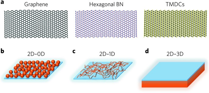
ABSTRACT The isolation of a growing number of two-dimensional (2D) materials has inspired worldwide efforts to integrate distinct 2D materials into van der Waals (vdW) heterostructures.
Given that any passivated, dangling-bond-free surface will interact with another through vdW forces, the vdW heterostructure concept can be extended to include the integration of 2D
materials with non-2D materials that adhere primarily through non-covalent interactions. We present a succinct and critical survey of emerging mixed-dimensional (2D + _n_D, where _n_ is 0, 1
or 3) heterostructure devices. By comparing and contrasting with all-2D vdW heterostructures as well as with competing conventional technologies, we highlight the challenges and
opportunities for mixed-dimensional vdW heterostructures. Access through your institution Buy or subscribe This is a preview of subscription content, access via your institution ACCESS
OPTIONS Access through your institution Subscribe to this journal Receive 12 print issues and online access $259.00 per year only $21.58 per issue Learn more Buy this article * Purchase on
SpringerLink * Instant access to full article PDF Buy now Prices may be subject to local taxes which are calculated during checkout ADDITIONAL ACCESS OPTIONS: * Log in * Learn about
institutional subscriptions * Read our FAQs * Contact customer support SIMILAR CONTENT BEING VIEWED BY OTHERS VAN DER WAALS HETEROSTRUCTURES Article 28 July 2022 VAN DER WAALS DEVICE
INTEGRATION BEYOND THE LIMITS OF VAN DER WAALS FORCES USING ADHESIVE MATRIX TRANSFER Article 08 December 2023 UNDERSTANDING EPITAXIAL GROWTH OF TWO-DIMENSIONAL MATERIALS AND THEIR
HOMOSTRUCTURES Article 10 July 2024 REFERENCES * Novoselov, K. S. et al. Electric field effect in atomically thin carbon films. _Science_ 306, 666–669 (2004). CAS Google Scholar *
Jariwala, D., Sangwan, V. K., Lauhon, L. J., Marks, T. J. & Hersam, M. C. Emerging device applications for semiconducting two-dimensional transition metal dichalcogenides. _ACS Nano_ 8,
1102–1120 (2014). CAS Google Scholar * Britnell, L. et al. Field-effect tunneling transistor based on vertical graphene heterostructures. _Science_ 335, 947–950 (2012). CAS Google Scholar
* Britnell, L. et al. Strong light–matter interactions in heterostructures of atomically thin films. _Science_ 340, 1311–1314 (2013). CAS Google Scholar * Georgiou, T. et al. Vertical
field-effect transistor based on graphene–WS2 heterostructures for flexible and transparent electronics. _Nature Nanotech._ 8, 100–103 (2013). CAS Google Scholar * Mishchenko, A. et al.
Twist-controlled resonant tunnelling in graphene/boron nitride/graphene heterostructures. _Nature Nanotech._ 9, 808–813 (2014). CAS Google Scholar * Yu, W. J. et al. Vertically stacked
multi-heterostructures of layered materials for logic transistors and complementary inverters. _Nature Mater._ 12, 246–252 (2012). Google Scholar * Yu, W. J. et al. Highly efficient
gate-tunable photocurrent generation in vertical heterostructures of layered materials. _Nature Nanotech._ 8, 952–958 (2013). CAS Google Scholar * Grigorieva, I. V. & Geim, A. K. Van
der Waals heterostructures. _Nature_ 499, 419–425 (2013). Google Scholar * Das, S., Robinson, J. A., Dubey, M., Terrones, H. & Terrones, M. Beyond graphene: progress in novel
two-dimensional materials and van der Waals solids. _Annu. Rev. Mater. Res._ 45, 1–27 (2015). CAS Google Scholar * Wang, H., Yuan, H., Sae Hong, S., Li, Y. & Cui, Y. Physical and
chemical tuning of two-dimensional transition metal dichalcogenides. _Chem. Soc. Rev._ 44, 2664–2680 (2015). CAS Google Scholar * Chhowalla, M. et al. The chemistry of two-dimensional
layered transition metal dichalcogenide nanosheets. _Nature Chem._ 5, 263–275 (2013). Google Scholar * Hoppe, H. & Sariciftci, N. S. Organic solar cells: an overview. _J. Mater. Res._
19, 1924–1945 (2004). CAS Google Scholar * Gong, M. et al. Polychiral semiconducting carbon nanotube–fullerene solar cells. _Nano Lett._ 14, 5308–5314 (2014). CAS Google Scholar * Neto,
A. C., Guinea, F., Peres, N., Novoselov, K. S. & Geim, A. K. The electronic properties of graphene. _Rev. Mod. Phys._ 81, 109–162 (2009). Google Scholar * Wang, Q. H., Kalantar-Zadeh,
K., Kis, A., Coleman, J. N. & Strano, M. S. Electronics and optoelectronics of two-dimensional transition metal dichalcogenides. _Nature Nanotech._ 7, 699–712 (2012). CAS Google Scholar
* Kroto, H. W., Heath, J. R., O'Brien, S. C., Curl, R. F. & Smalley, R. E. C60: buckminsterfullerene. _Nature_ 318, 162–163 (1985). CAS Google Scholar * Facchetti, A.
Semiconductors for organic transistors. _Mater. Today_ 10, 28–37 (2007). CAS Google Scholar * Alivisatos, A. P. Semiconductor clusters, nanocrystals, and quantum dots. _Science_ 271,
933–937 (1996). CAS Google Scholar * Arnold, M. S., Green, A. A., Hulvat, J. F., Stupp, S. I. & Hersam, M. C. Sorting carbon nanotubes by electronic structure using density
differentiation. _Nature Nanotech._ 1, 60–65 (2006). CAS Google Scholar * Lieber, C. M. & Wang, Z. L. Functional nanowires. _MRS Bull._ 32, 99–108 (2007). CAS Google Scholar * Yu,
X., Marks, T. J. & Facchetti, A. Metal oxides for optoelectronic applications. _Nature Mater._ 15, 383–396 (2016). CAS Google Scholar * Li, S.-L., Tsukagoshi, K., Orgiu, E. &
Samorì, P. Charge transport and mobility engineering in two-dimensional transition metal chalcogenide semiconductors. _Chem. Soc. Rev._ 45, 118–151 (2016). CAS Google Scholar * Kang, J.,
Liu, W., Sarkar, D., Jena, D. & Banerjee, K. Computational study of metal contacts to monolayer transition-metal dichalcogenide semiconductors. _Phys. Rev. X_ 4, 031005 (2014). Google
Scholar * Allain, A., Kang, J., Banerjee, K. & Kis, A. Electrical contacts to two-dimensional semiconductors. _Nature Mater._ 14, 1195–1205 (2015). CAS Google Scholar * Sze, S. M.
& Ng, K. K. _Physics of Semiconductor Devices_ 3rd edn (Wiley, 2007). Google Scholar * Ishii, H., Sugiyama, K., Ito, E. & Seki, K. Energy level alignment and interfacial electronic
structures at organic/metal and organic/organic interfaces. _Adv. Mater._ 11, 605–625 (1999). CAS Google Scholar * So, F. _Organic Electronics: Materials, Processing, Devices and
Applications_ (CRC, 2009). Google Scholar * Jariwala, D., Sangwan, V. K., Lauhon, L. J., Marks, T. J. & Hersam, M. C. Carbon nanomaterials for electronics, optoelectronics,
photovoltaics, and sensing. _Chem. Soc. Rev._ 42, 2824–2860 (2013). CAS Google Scholar * Wang, Q. H. & Hersam, M. C. Room-temperature molecular-resolution characterization of
self-assembled organic monolayers on epitaxial graphene. _Nature Chem._ 1, 206–211 (2009). CAS Google Scholar * Kufer, D. et al. Hybrid 2D–0D MoS2–PbS quantum dot photodetectors. _Adv.
Mater._ 27, 176–180 (2015). CAS Google Scholar * Konstantatos, G. et al. Hybrid graphene-quantum dot phototransistors with ultrahigh gain. _Nature Nanotech._ 7, 363–368 (2012). CAS Google
Scholar * Jariwala, D. et al. Large-area, low-voltage, antiambipolar heterojunctions from solution-processed semiconductors. _Nano Lett._ 15, 416–421 (2015). CAS Google Scholar *
Jariwala, D. et al. Gate-tunable carbon nanotube–MoS2 heterojunction p–n diode. _Proc. Natl Acad. Sci. USA_ 110, 18076–18080 (2013). CAS Google Scholar * Lee, J.-H. et al. Wafer-scale
growth of single-crystal monolayer graphene on reusable hydrogen-terminated germanium. _Science_ 344, 286–289 (2014). CAS Google Scholar * Ruzmetov, D. et al. Vertical 2D/3D semiconductor
heterostructures based on epitaxial molybdenum disulfide and gallium nitride. _ACS Nano_ 10, 3580–3588 (2016). CAS Google Scholar * Chung, K., Lee, C.-H. & Yi, G.-C. Transferable GaN
layers grown on ZnO-coated graphene layers for optoelectronic devices. _Science_ 330, 655–657 (2010). CAS Google Scholar * Kobayashi, Y., Kumakura, K., Akasaka, T. & Makimoto, T.
Layered boron nitride as a release layer for mechanical transfer of GaN-based devices. _Nature_ 484, 223–227 (2012). CAS Google Scholar * Kory, M. J. et al. Gram-scale synthesis of
two-dimensional polymer crystals and their structure analysis by X-ray diffraction. _Nature Chem._ 6, 779–784 (2014). CAS Google Scholar * Pfeffermann, M. et al. Free-standing monolayer
two-dimensional supramolecular organic framework with good internal order. _J. Am. Chem. Soc._ 137, 14525–14532 (2015). CAS Google Scholar * Kissel, P., Murray, D. J., Wulftange, W. J.,
Catalano, V. J. & King, B. T. A nanoporous two-dimensional polymer by single-crystal-to-single-crystal photopolymerization. _Nature Chem._ 6, 774–778 (2014). CAS Google Scholar *
Zhuang, X. et al. Conjugated microporous polymers with dimensionality-controlled heterostructures for green energy devices. _Adv. Mater._ 27, 3789–3796 (2015). CAS Google Scholar * Murray,
D. J. et al. Large area synthesis of a nanoporous two-dimensional polymer at the air/water interface. _J. Am. Chem. Soc._ 137, 3450–3453 (2015). CAS Google Scholar * Tour, J. M. Molecular
electronics. synthesis and testing of components. _Acc. Chem. Res._ 33, 791–804 (2000). CAS Google Scholar * Lee C.-H. et al. Epitaxial growth of molecular crystals on van der Waals
substrates for high-performance organic electronics. _Adv. Mater._ 26, 2812–2817 (2014). CAS Google Scholar * Kang, S. J. et al. Organic field effect transistors based on graphene and
hexagonal boron nitride heterostructures. _Adv. Funct. Mater._ 24, 5157–5163 (2014). CAS Google Scholar * Lee, G.-H. et al. Heterostructures based on inorganic and organic van der Waals
systems. _APL Mater._ 2, 092511 (2014). Google Scholar * Jo, S. B. et al. Boosting photon harvesting in organic solar cells with highly oriented molecular crystals via graphene–organic
heterointerface. _ACS Nano_ 9, 8206–8219 (2015). CAS Google Scholar * Lee, W. H. et al. Surface-directed molecular assembly of pentacene on monolayer graphene for high-performance organic
transistors. _J. Am. Chem. Soc._ 133, 4447–4454 (2011). CAS Google Scholar * Lee, S. et al. Enhanced characteristics of pentacene field-effect transistors with graphene electrodes and
substrate treatments. _Appl. Phys. Lett._ 99, 083306 (2011). Google Scholar * Lee, S. et al. Enhanced charge injection in pentacene field-effect transistors with graphene electrodes. _Adv.
Mater._ 23, 100–105 (2011). CAS Google Scholar * Basu, S., Lee, M. C. & Wang, Y.-H. Graphene-based electrodes for enhanced organic thin film transistors based on pentacene. _Phys.
Chem. Chem. Phys._ 16, 16701–16710 (2014). CAS Google Scholar * Di, C.-A. et al. Patterned graphene as source/drain electrodes for bottom-contact organic field-effect transistors. _Adv.
Mater._ 20, 3289–3293 (2008). CAS Google Scholar * Wang, Y. et al. Graphene-assisted solution growth of vertically oriented organic semiconducting single crystals. _ACS Nano_ 9, 9486–9496
(2015). CAS Google Scholar * Colson, J. W. et al. Oriented 2D. _Science_, 332, 228–231 (2011). CAS Google Scholar * Huafeng, Y. et al. Dielectric nanosheets made by liquid-phase
exfoliation in water and their use in graphene-based electronics. _2D Mater._ 1, 011012 (2014). Google Scholar * Schlierf, A. et al. Nanoscale insight into the exfoliation mechanism of
graphene with organic dyes: effect of charge, dipole and molecular structure. _Nanoscale_ 5, 4205–4216 (2013). CAS Google Scholar * Sarbani, B., Feri, A. & Yeong-Her, W. Blending
effect of 6,13-bis(triisopropylsilylethynyl) pentacene–graphene composite layers for flexible thin film transistors with a polymer gate dielectric. _Nanotechnology_ 25, 085201 (2014). Google
Scholar * Zhang, Y. et al. Two-dimensional MoS2-assisted immediate aggregation of poly-3-hexylthiophene with high mobility. _Phys. Chem. Chem. Phys._ 17, 27565–27572 (2015). CAS Google
Scholar * He, D. et al. Two-dimensional quasi-freestanding molecular crystals for high-performance organic field-effect transistors. _Nature Commun._ 5, 5162 (2014). CAS Google Scholar *
Parui, S. et al. Gate-controlled energy barrier at a graphene/molecular semiconductor junction. _Adv. Funct. Mater._ 25, 2972–2979 (2015). CAS Google Scholar * Liu, Y., Zhou, H., Weiss, N.
O., Huang, Y. & Duan, X. High-performance organic vertical thin film transistor using graphene as a tunable contact. _ACS Nano_ 9, 11102–11108 (2015). CAS Google Scholar * Hlaing, H.
et al. Low-voltage organic electronics based on a gate-tunable injection barrier in vertical graphene-organic semiconductor heterostructures. _Nano Lett._ 15, 69–74 (2015). CAS Google
Scholar * Nomura, K. et al. Room-temperature fabrication of transparent flexible thin-film transistors using amorphous oxide semiconductors. _Nature_ 432, 488–492 (2004). CAS Google
Scholar * Liu, Y. et al. Highly flexible electronics from scalable vertical thin film transistors. _Nano Lett._ 14, 1413–1418 (2014). CAS Google Scholar * Heo, J. et al. Graphene and
thin-film semiconductor heterojunction transistors integrated on wafer scale for low-power electronics. _Nano Lett._ 13, 5967–5971 (2013). CAS Google Scholar * Yang, H. et al. Graphene
barristor, a triode device with a gate-controlled Schottky barrier. _Science_ 336, 1140–1143 (2012). CAS Google Scholar * Ojeda-Aristizabal, C., Bao, W. & Fuhrer, M. S. Thin-film
barristor: a gate-tunable vertical graphene–pentacene device. _Phys. Rev. B_ 88, 035435 (2013). Google Scholar * Jariwala, D. et al. Hybrid, gate-tunable, van der Waals p–n heterojunctions
from pentacene and MoS2 . _Nano Lett._ 16, 497–503 (2016). CAS Google Scholar * Velez, S. et al. Gate-tunable diode and photovoltaic effect in an organic–2D layered material p–n junction.
_Nanoscale_ 7, 15442–15449 (2015). CAS Google Scholar * Jeong, H. et al. Semiconductor–insulator–semiconductor diode consisting of monolayer MoS2, h-BN, and GaN heterostructure. _ACS Nano_
9, 10032–10038 (2015). CAS Google Scholar * Sarkar, D. et al. A subthermionic tunnel field-effect transistor with an atomically thin channel. _Nature_ 526, 91–95 (2015). CAS Google
Scholar * Vaziri, S. et al. Going ballistic: graphene hot electron transistors. _Solid State Commun._ 224, 64–75 (2015). CAS Google Scholar * Mehr, W. et al. Vertical graphene base
transistor. _IEEE Electron Device Lett._ 33, 691–693 (2012). CAS Google Scholar * Vaziri, S. et al. A graphene-based hot electron transistor. _Nano Lett._ 13, 1435–1439 (2013). CAS Google
Scholar * Torres, C. M. et al. High-current gain two-dimensional MoS2-base hot-electron transistors. _Nano Lett._ 15, 7905–7912 (2015). CAS Google Scholar * Vaziri, S. et al. Bilayer
insulator tunnel barriers for graphene-based vertical hot-electron transistors. _Nanoscale_ 7, 13096–13104 (2015). CAS Google Scholar * Mead, C. A. Operation of tunnel-emission devices.
_J. Appl. Phys._ 32, 646–652 (1961). Google Scholar * van 't Erve, O. M. J. et al. Low-resistance spin injection into silicon using graphene tunnel barriers. _Nature Nanotech._ 7,
737–742 (2012). CAS Google Scholar * van 't Erve O. M. J. et al. Spin transport and Hanle effect in silicon nanowires using graphene tunnel barriers. _Nature Commun._ 6, 7541 (2015).
CAS Google Scholar * Koppens F. H. L. et al. Photodetectors based on graphene, other two-dimensional materials and hybrid systems. _Nature Nanotech._ 9, 780–793 (2014). CAS Google Scholar
* Sun, Z. et al. Infrared photodetectors based on CVD-grown graphene and PbS quantum dots with ultrahigh responsivity. _Adv. Mater._ 24, 5878–5883 (2012). CAS Google Scholar * Jang, S.,
Hwang, E., Lee, Y., Lee, S. & Cho, J. H. Multifunctional graphene optoelectronic devices capable of detecting and storing photonic signals. _Nano Lett._ 15, 2542–2547 (2015). CAS Google
Scholar * Roy, K. et al. Graphene-MoS2 hybrid structures for multifunctional photoresponsive memory devices. _Nature Nanotech._ 8, 826–830 (2013). CAS Google Scholar * Yu, S. H. et al.
Dye-sensitized MoS2 photodetector with enhanced spectral photoresponse. _ACS Nano_ 8, 8285–8291 (2014). CAS Google Scholar * Cho, E. et al. Enhancement of photoresponsive electrical
characteristics of multilayer MoS2 transistors using rubrene patches. _Nano Res._ 8, 790–800 (2015). CAS Google Scholar * An, X., Liu, F., Jung, Y. J. & Kar, S. Tunable
graphene–silicon heterojunctions for ultrasensitive photodetection. _Nano Lett._ 13, 909–916 (2013). CAS Google Scholar * Zeng, L.-H. et al. Monolayer graphene/germanium Schottky junction
as high-performance self-driven infrared light photodetector. _ACS Appl. Mater. Interfaces_ 5, 9362–9366 (2013). CAS Google Scholar * Chen, C.-C., Aykol, M., Chang, C.-C., Levi, A. F. J.
& Cronin, S. B. Graphene–silicon Schottky diodes. _Nano Lett._ 11, 1863–1867 (2011). CAS Google Scholar * Zhu, M. et al. Vertical junction photodetectors based on reduced graphene
oxide/silicon Schottky diodes. _Nanoscale_ 6, 4909–4914 (2014). CAS Google Scholar * An, Y., Behnam, A., Pop, E. & Ural, A. Metal–semiconductor–metal photodetectors based on
graphene/p-type silicon Schottky junctions. _Appl. Phys. Lett._ 102, 013110 (2013). Google Scholar * Nie, B. et al. Monolayer graphene film on ZnO nanorod array for high-performance
Schottky junction ultraviolet photodetectors. _Small_ 9, 2872–2879 (2013). CAS Google Scholar * Gao, Z. et al. Self-powered flexible and transparent photovoltaic detectors based on CdSe
nanobelt/graphene Schottky junctions. _Nanoscale_ 5, 5576–5581 (2013). CAS Google Scholar * Shin, D. H. et al. Graphene/Si-quantum-dot heterojunction diodes showing high photosensitivity
compatible with quantum confinement effect. _Adv. Mater._ 27, 2614–2620 (2015). CAS Google Scholar * Miao, J. et al. High-responsivity graphene/InAs nanowire heterojunction near-infrared
photodetectors with distinct photocurrent on/off ratios. _Small_ 11, 936–942 (2015). CAS Google Scholar * Esmaeili-Rad, M. R. & Salahuddin, S. High performance molybdenum disulfide
amorphous silicon heterojunction photodetector. _Sci. Rep._ 3, 2345 (2013). Google Scholar * Liu, F. et al. Van der Waals p–n junction based on an organic–inorganic heterostructure. _Adv.
Funct. Mater._ 25, 5865–5871 (2015). CAS Google Scholar * Koester, S. J. & Li, M. Waveguide-coupled graphene optoelectronics. _IEEE J. Sel. Top. Quant. Electron._ 20, 84–94 (2014).
Google Scholar * Furchi, M. et al. Microcavity-integrated graphene photodetector. _Nano Lett._ 12, 2773–2777 (2012). CAS Google Scholar * Liu, M. et al. A graphene-based broadband optical
modulator. _Nature_ 474, 64–67 (2011). CAS Google Scholar * Pospischil, A. et al. CMOS-compatible graphene photodetector covering all optical communication bands. _Nature Photon._ 7,
892–896 (2013). CAS Google Scholar * Gan, X. et al. Chip-integrated ultrafast graphene photodetector with high responsivity. _Nature Photon._ 7, 883–887 (2013). CAS Google Scholar *
Shiue, R.-J. et al. High-responsivity graphene–boron nitride photodetector and autocorrelator in a silicon photonic integrated circuit. _Nano Lett._ 15, 7288–7293 (2015). CAS Google Scholar
* Wang, X., Cheng, Z., Xu, K., Tsang, H. K. & Xu, J.-B. High-responsivity graphene/silicon-heterostructure waveguide photodetectors. _Nature Photon._ 7, 888–891 (2013). CAS Google
Scholar * Li, X. et al. Graphene-on-silicon Schottky junction solar cells. _Adv. Mater._ 22, 2743–2748 (2010). CAS Google Scholar * Brus, V. V. et al. Stability of graphene–silicon
heterostructure solar cells. _Phys. Status Solidi A_ 211, 843–847 (2014). CAS Google Scholar * Shi, E. et al. Colloidal antireflection coating improves graphene–silicon solar cells. _Nano
Lett._ 13, 1776–1781 (2013). CAS Google Scholar * Miao, X. et al. High efficiency graphene solar cells by chemical doping. _Nano Lett._ 12, 2745–2750 (2012). CAS Google Scholar * Lin, Y.
et al. Graphene/semiconductor heterojunction solar cells with modulated antireflection and graphene work function. _Energ. Environ. Sci._ 6, 108–115 (2013). CAS Google Scholar * Zhang, X.
et al. High-efficiency graphene/Si nanoarray Schottky junction solar cells via surface modification and graphene doping. _J. Mater. Chem. A_, 1, 6593–6601 (2013). CAS Google Scholar *
Feng, T. et al. Graphene based Schottky junction solar cells on patterned silicon-pillar-array substrate. _Appl. Phys. Lett._ 99, 233505 (2011). Google Scholar * Xie, C. et al. Monolayer
graphene film/silicon nanowire array Schottky junction solar cells. _Appl. Phys. Lett._ 99, 133113 (2011). Google Scholar * Song, Y. et al. Role of interfacial oxide in high-efficiency
graphene–silicon Schottky barrier solar cells. _Nano Lett._ 15, 2104–2110 (2015). CAS Google Scholar * Li, X. et al. 18.5% efficient graphene/GaAs van der Waals heterostructure solar cell.
_Nano Energy_, 16, 310–319 (2015). CAS Google Scholar * Vazquez-Mena, O. et al. Performance enhancement of a graphene–zinc phosphide solar cell using the electric field-effect. _Nano
Lett._ 14, 4280–4285 (2014). CAS Google Scholar * Zhang, L. et al. Graphene–CdSe nanobelt solar cells with tunable configurations. _Nano Res._ 4, 891–900 (2011). CAS Google Scholar * Ye,
Y. et al. A simple and scalable graphene patterning method and its application in CdSe nanobelt/graphene Schottky junction solar cells. _Nanoscale_ 3, 1477–1481 (2011). CAS Google Scholar
* Lin, S. et al. Graphene/CdTe heterostructure solar cell and its enhancement with photo-induced doping. _Appl. Phys. Lett._ 107, 191106 (2015). Google Scholar * Ye, Y. & Dai, L.
Graphene-based Schottky junction solar cells. _J. Mater. Chem._ 22, 24224–24229 (2012). CAS Google Scholar * Lopez-Sanchez, O. et al. Light generation and harvesting in a van der Waals
heterostructure. _ACS Nano_ 8, 3042–3048 (2014). CAS Google Scholar * Tsai, M.-L. et al. Monolayer MoS2 heterojunction solar cells. _ACS Nano_ 8, 8317–8322 (2014). CAS Google Scholar *
Lin, S. et al. Interface designed MoS2/GaAs heterostructure solar cell with sandwich stacked hexagonal boron nitride. _Sci. Rep._ 5, 15103 (2015). CAS Google Scholar * Liu, X. et al.
Strong light–matter coupling in two-dimensional atomic crystals. _Nature Photon._ 9, 30–34 (2015). CAS Google Scholar * Tan, Y. et al. Polarization-dependent optical absorption of MoS2 for
refractive index sensing. _Sci. Rep._ 4, 7523 (2014). CAS Google Scholar * Mak, K. F., Lee, C., Hone, J., Shan, J. & Heinz, T. F. Atomically thin MoS2: a new direct-gap semiconductor.
_Phys. Rev. Lett._ 105, 136805 (2010). Google Scholar * Splendiani, A. et al. Emerging photoluminescence in monolayer MoS2 . _Nano Lett._ 10, 1271–1275 (2010). CAS Google Scholar *
Cheng, R. et al. Electroluminescence and photocurrent generation from atomically sharp WSe2/MoS2 heterojunction p–n diodes. _Nano Lett._ 14, 5590–5597 (2014). CAS Google Scholar * Withers,
F. et al. Light-emitting diodes by band-structure engineering in van der Waals heterostructures. _Nature Mater._ 14, 301–306 (2015). CAS Google Scholar * Ye, Y. et al. Exciton-dominant
electroluminescence from a diode of monolayer MoS2 . _Appl. Phys. Lett._ 104, 193508 (2014). Google Scholar * Li, D. et al. Electric-field-induced strong enhancement of electroluminescence
in multilayer molybdenum disulfide. _Nature Commun._ 6, 7509 (2015). Google Scholar * Lee, C.-H. et al. Flexible inorganic nanostructure light-emitting diodes fabricated on graphene films.
_Adv. Mater._ 23, 4614–4619 (2011). CAS Google Scholar * Ye, Y. et al. Multicolor graphene nanoribbon/semiconductor nanowire heterojunction light-emitting diodes. _J. Mater. Chem._ 21,
11760–11763 (2011). CAS Google Scholar * Han, T.-H. et al. Extremely efficient flexible organic light-emitting diodes with modified graphene anode. _Nature Photon._ 6, 105–110 (2012). CAS
Google Scholar * Han, N. et al. Improved heat dissipation in gallium nitride light-emitting diodes with embedded graphene oxide pattern. _Nature Commun._ 4, 1452 (2013). Google Scholar *
Amani, M. et al. Near-unity photoluminescence quantum yield in MoS2 . _Science_ 350, 1065–1068 (2015). CAS Google Scholar * Dou, L. et al. Atomically thin two-dimensional
organic–inorganic hybrid perovskites. _Science_ 349, 1518–1521 (2015). CAS Google Scholar * Callahan, D. M., Munday, J. N. & Atwater, H. A. Solar cell light trapping beyond the ray
optic limit. _Nano Lett._ 12, 214–218 (2012). CAS Google Scholar * Ye, Y. et al. Monolayer excitonic laser. _Nature Photon._ 9, 733–737 (2015). CAS Google Scholar * Wu, S. et al.
Monolayer semiconductor nanocavity lasers with ultralow thresholds. _Nature_ 520, 69–72 (2015). CAS Google Scholar * Kang, K. et al. High-mobility three-atom-thick semiconducting films
with wafer-scale homogeneity. _Nature_ 520, 656–660 (2015). CAS Google Scholar Download references ACKNOWLEDGEMENTS We acknowledge support from the Materials Research Science and
Engineering Center (MRSEC) of Northwestern University (NSF DMR-1121262), and the 2-DARE programme (NSF EFRI-143510). AUTHOR INFORMATION Author notes * Deep Jariwala Present address: Present
address: Department of Applied Physics and Materials Science, California Institute of Technology, Pasadena, California 91125, USA, AUTHORS AND AFFILIATIONS * Department of Materials Science
and Engineering, Northwestern University, Evanston, 60208, Illinois, USA Deep Jariwala, Tobin J. Marks & Mark C. Hersam * Department of Chemistry, Northwestern University, Evanston,
60208, Illinois, USA Tobin J. Marks & Mark C. Hersam Authors * Deep Jariwala View author publications You can also search for this author inPubMed Google Scholar * Tobin J. Marks View
author publications You can also search for this author inPubMed Google Scholar * Mark C. Hersam View author publications You can also search for this author inPubMed Google Scholar
CORRESPONDING AUTHOR Correspondence to Mark C. Hersam. ETHICS DECLARATIONS COMPETING INTERESTS The authors declare no competing financial interests. RIGHTS AND PERMISSIONS Reprints and
permissions ABOUT THIS ARTICLE CITE THIS ARTICLE Jariwala, D., Marks, T. & Hersam, M. Mixed-dimensional van der Waals heterostructures. _Nature Mater_ 16, 170–181 (2017).
https://doi.org/10.1038/nmat4703 Download citation * Received: 19 February 2016 * Accepted: 21 June 2016 * Published: 01 August 2016 * Issue Date: February 2017 * DOI:
https://doi.org/10.1038/nmat4703 SHARE THIS ARTICLE Anyone you share the following link with will be able to read this content: Get shareable link Sorry, a shareable link is not currently
available for this article. Copy to clipboard Provided by the Springer Nature SharedIt content-sharing initiative