Play all audios:
ABSTRACT The nitrogen-vacancy defect centre in diamond1,2,3,4 has potential applications in nanoscale electric and magnetic-field sensing2,3,4,5,6, single-photon microscopy7,8, quantum
information processing9 and bioimaging10. These applications rely on the ability to position a single nitrogen-vacancy centre within a few nanometres of a sample, and then scan it across the
sample surface, while preserving the centre's spin coherence and readout fidelity. However, existing scanning techniques, which use a single diamond nanocrystal grafted onto the tip of
a scanning probe microscope2,8,11,12, suffer from short spin coherence times due to poor crystal quality, and from inefficient far-field collection of the fluorescence from the
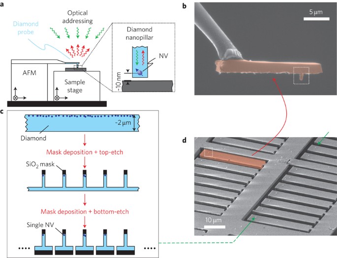
nitrogen-vacancy centre. Here, we demonstrate a robust method for scanning a single nitrogen-vacancy centre within tens of nanometres from a sample surface that addresses both of these
concerns. This is achieved by positioning a single nitrogen-vacancy centre at the end of a high-purity diamond nanopillar, which we use as the tip of an atomic force microscope. Our approach
ensures long nitrogen-vacancy spin coherence times (∼75 µs), enhanced nitrogen-vacancy collection efficiencies due to waveguiding, and mechanical robustness of the device (several weeks of
scanning time). We are able to image magnetic domains with widths of 25 nm, and demonstrate a magnetic field sensitivity of 56 nT Hz–1/2 at a frequency of 33 kHz, which is unprecedented for
scanning nitrogen-vacancy centres. Access through your institution Buy or subscribe This is a preview of subscription content, access via your institution ACCESS OPTIONS Access through your
institution Subscribe to this journal Receive 12 print issues and online access $259.00 per year only $21.58 per issue Learn more Buy this article * Purchase on SpringerLink * Instant access
to full article PDF Buy now Prices may be subject to local taxes which are calculated during checkout ADDITIONAL ACCESS OPTIONS: * Log in * Learn about institutional subscriptions * Read
our FAQs * Contact customer support SIMILAR CONTENT BEING VIEWED BY OTHERS NANOSCALE ELECTRIC FIELD IMAGING WITH AN AMBIENT SCANNING QUANTUM SENSOR MICROSCOPE Article Open access 09
September 2022 NANOSCALE ELECTRIC-FIELD IMAGING BASED ON A QUANTUM SENSOR AND ITS CHARGE-STATE CONTROL UNDER AMBIENT CONDITION Article Open access 28 April 2021 WIDE-FIELD MAGNETOMETRY USING
NITROGEN-VACANCY COLOR CENTERS WITH RANDOMLY ORIENTED MICRO-DIAMONDS Article Open access 26 October 2022 REFERENCES * Chernobrod, B. M. & Berman, G. P. Spin microscope based on
optically detected magnetic resonance. _J. Appl. Phys._ 97, 014903 (2005). Article Google Scholar * Balasubramanian, G. et al. Nanoscale imaging magnetometry with diamond spins under
ambient conditions. _Nature_ 455, 648–651 (2008). Article CAS Google Scholar * Maze, J. R. et al. Nanoscale magnetic sensing with an individual electronic spin in diamond. _Nature_ 455,
644–647 (2008). Article CAS Google Scholar * Taylor, J. et al. High-sensitivity diamond magnetometer with nanoscale resolution. _Nature Phys._ 4, 810–816 (2008). Article CAS Google
Scholar * Dolde, F. et al. Electric-field sensing using single diamond spins. _Nature Phys._ 7, 459–463 (2011). Article CAS Google Scholar * Degen, C. L. Scanning magnetic field
microscope with a diamond single-spin sensor. _Appl. Phys. Lett._ 92, 243111 (2008). Article Google Scholar * Sekatskii, S. & Letokhov, V. Nanometer-resolution scanning optical
microscope with resonance excitation of the fluorescence of the samples from a single-atom excited center. _JETP Lett._ 63, 319–323 (1996). Article Google Scholar * Cuche, A. et al.
Near-field optical microscopy with a nanodiamond-based single-photon tip. _Opt. Express_ 17, 19969–19980 (2009). Article CAS Google Scholar * Neumann, P. et al. Quantum register based on
coupled electron spins in a room-temperature solid. _Nature Phys._ 6, 249–253 (2010). Article CAS Google Scholar * McGuinness, L. P. et al. Quantum measurement and orientation tracking of
fluorescent nanodiamonds inside living cells. _Nature Nanotech._ 6, 358–363 (2011). Article CAS Google Scholar * Kuhn, S., Hettich, C., Schmitt, C., Poizat, J. & Sandoghdar, V.
Diamond colour centres as a nanoscopic light source for scanning near-field optical microscopy. _J. Microsc._ 202, 2–6 (2001). Article CAS Google Scholar * Rondin, L. et al. Nanoscale
magnetic field mapping with a single spin scanning probe magnetometer. _Appl. Phys. Lett._ (in the press). * Kurtsiefer, C., Mayer, S., Zarda, P. & Weinfurter, H. Stable solid-state
source of single photons. _Phys. Rev. Lett._ 85, 290–293 (2000). Article CAS Google Scholar * Balasubramanian, G. et al. Ultralong spin coherence time in isotopically engineered diamond.
_Nature Mater._ 8, 383–387 (2009). Article CAS Google Scholar * Gruber, A. et al. Scanning confocal optical microscopy and magnetic resonance on single defect centers. _Science_ 276,
2012–2014 (1997). Article CAS Google Scholar * Michaelis, J., Hettich, C., Mlynek, J. & Sandoghdar, V. Optical microscopy using a single-molecule light source. _Nature_ 405, 325–328
(2000). Article CAS Google Scholar * Kalish, R. et al. Nitrogen doping of diamond by ion implantation. _Diamond Relat. Mater._ 6, 516–520 (1997). Article CAS Google Scholar * Babinec,
T. M. et al. A diamond nanowire single-photon source. _Nature Nanotech._ 5, 195–199 (2010). Article CAS Google Scholar * Hausmann, B. J. et al. Fabrication of diamond nanowires for
quantum information processing applications. _Diamond Relat. Mater._ 19, 621–629 (2010). Article CAS Google Scholar * Jelezko, F., Gaebel, T., Popa, I., Gruber, A. & Wrachtrup, J.
Observation of coherent oscillations in a single electron spin. _Phys. Rev. Lett._ 92, 076401 (2004). Article CAS Google Scholar * Van Oort, E. & Glasbeek, M. Optically detected low
field electron spin echo envelope modulations of fluorescent N-V centers in diamond. _Chem. Phys._ 143, 131–140 (1990). Article CAS Google Scholar * De Lange, G., Ristè, D., Dobrovitski,
V. V. & Hanson, R. Single-spin magnetometry with multipulse sensing sequences. _Phys. Rev. Lett._ 106, 080802 (2011). Article CAS Google Scholar * Dreau, A. et al. Avoiding power
broadening in optically detected magnetic resonance of single NV defects for enhanced dc magnetic field sensitivity. _Phys. Rev. B_ 84, 195204 (2011). Article Google Scholar * Grinolds, M.
S. et al. Quantum control of proximal spins using nanoscale magnetic resonance imaging. _Nature Phys._ 7, 687–692 (2011). Article CAS Google Scholar * Lai, N., Zheng, D., Jelezko, F.,
Treussart, F. & Roch, J-F. Influence of a static magnetic field on the photoluminescence of an ensemble of nitrogen-vacancy color centers in a diamond single-crystal. _Appl. Phys. Lett._
95, 133101 (2009). Article Google Scholar * Buchler, B. C., Kalkbrenner, T., Hettich, C. & Sandoghdar, V. Measuring the quantum efficiency of the optical emission of single radiating
dipoles using a scanning mirror. _Phys. Rev. Lett._ 95, 063003 (2005). Article CAS Google Scholar * Bradac, C. et al. Observation and control of blinking nitrogen-vacancy centres in
discrete nanodiamonds. _Nature Nanotech._ 5, 345–349 (2010). Article CAS Google Scholar * Pezzagna, S. et al. Nanoscale engineering and optical addressing of single spins in diamond.
_Small_ 6, 2117–2121 (2010). Article CAS Google Scholar * Naydenov, B. et al. Increasing the coherence time of single electron spins in diamond by high temperature annealing. _Appl. Phys.
Lett._ 97, 242511 (2010). Article Google Scholar * Wolny, F. et al. Iron filled carbon nanotubes as novel monopole-like sensors for quantitative magnetic force microscopy.
_Nanotechnology_ 21, 435501 (2010). Article CAS Google Scholar * Kohashi, T., Konoto, M. & Koike, K. High-resolution spin-polarized scanning electron microscopy (spin SEM). _J.
Electron Microsc._ 59, 43–52 (2010). Article CAS Google Scholar * Kane, B. E. A silicon-based nuclear spin quantum computer. _Nature_ 393, 133–137 (1998). Article CAS Google Scholar *
Recher, P. & Trauzettel, B. Quantum dots and spin qubits in graphene. _Nanotechnology_ 21, 302001 (2010). Article Google Scholar * Togan, E. et al. Quantum entanglement between an
optical photon and a solid-state spin qubit. _Nature_ 466, 730–734 (2010). Article CAS Google Scholar * Lee, C., Gu, E., Dawson, M., Friel, I. & Scarsbrook, G. Etching and
micro-optics fabrication in diamond using chlorine-based inductively-coupled plasma. _Diamond Relat. Mater._ 17, 1292–1296 (2008). Article CAS Google Scholar * Childress, L. et al.
Coherent dynamics of coupled electron and nuclear spin qubits in diamond. _Science_ 314, 281–285 (2006). Article CAS Google Scholar Download references ACKNOWLEDGEMENTS The authors thank
B.D. Terris and N. Supper from Hitachi GST for providing the magnetic recording samples. P.M. acknowledges support from the Swiss National Science Foundation and S.H. thanks the Kwanjeong
Scholarship Foundation for funding. M.S.G. is supported by fellowships from the Department of Defense (NDSEG programme) and the National Science Foundation (NSF). This work was supported by
NIST and DARPA QuEST and QuASAR programmes and in part was performed at the Center for Nanoscale Systems (CNS), a member of the National Nanotechnology Infrastructure Network (NNIN), which
is supported by the NSF (under award no. ECS–0335765). CNS is part of Harvard University. AUTHOR INFORMATION Author notes * P. Maletinsky, S. Hong and M. S. Grinolds: These authors
contributed equally to this work AUTHORS AND AFFILIATIONS * Department of Physics, Harvard University, Cambridge, 02138, Massachusetts, USA P. Maletinsky, M. S. Grinolds, M. D. Lukin, R. L.
Walsworth & A. Yacoby * School of Engineering and Applied Science, Harvard University, Cambridge, 02138, Massachusetts, USA S. Hong, B. Hausmann & M. Loncar * Harvard–Smithsonian
Center for Astrophysics, Cambridge, 02138, Massachusetts, USA R. L. Walsworth Authors * P. Maletinsky View author publications You can also search for this author inPubMed Google Scholar *
S. Hong View author publications You can also search for this author inPubMed Google Scholar * M. S. Grinolds View author publications You can also search for this author inPubMed Google
Scholar * B. Hausmann View author publications You can also search for this author inPubMed Google Scholar * M. D. Lukin View author publications You can also search for this author inPubMed
Google Scholar * R. L. Walsworth View author publications You can also search for this author inPubMed Google Scholar * M. Loncar View author publications You can also search for this
author inPubMed Google Scholar * A. Yacoby View author publications You can also search for this author inPubMed Google Scholar CONTRIBUTIONS All authors contributed to all aspects of this
work. CORRESPONDING AUTHOR Correspondence to A. Yacoby. ETHICS DECLARATIONS COMPETING INTERESTS The authors declare no competing financial interests. SUPPLEMENTARY INFORMATION SUPPLEMENTARY
INFORMATION Supplementary information (PDF 672 kb) RIGHTS AND PERMISSIONS Reprints and permissions ABOUT THIS ARTICLE CITE THIS ARTICLE Maletinsky, P., Hong, S., Grinolds, M. _et al._ A
robust scanning diamond sensor for nanoscale imaging with single nitrogen-vacancy centres. _Nature Nanotech_ 7, 320–324 (2012). https://doi.org/10.1038/nnano.2012.50 Download citation *
Received: 08 February 2012 * Accepted: 13 March 2012 * Published: 15 April 2012 * Issue Date: May 2012 * DOI: https://doi.org/10.1038/nnano.2012.50 SHARE THIS ARTICLE Anyone you share the
following link with will be able to read this content: Get shareable link Sorry, a shareable link is not currently available for this article. Copy to clipboard Provided by the Springer
Nature SharedIt content-sharing initiative