Play all audios:
ABSTRACT The development of new, high-quality functional materials has been at the forefront of condensed-matter research. The recent advent of two-dimensional black phosphorus has greatly
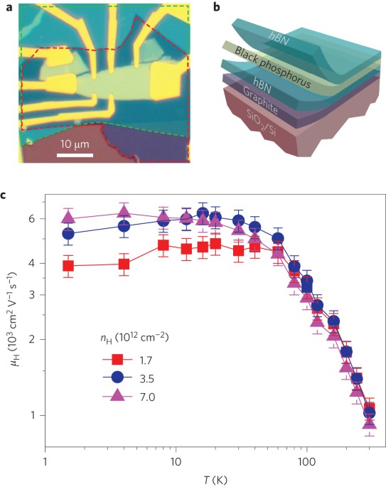
enriched the materials base of two-dimensional electron systems (2DESs)1,2,3,4,5. Here, we report the observation of the integer quantum Hall effect in a high-quality black phosphorus 2DES.
The high quality is achieved by embedding the black phosphorus 2DES in a van der Waals heterostructure close to a graphite back gate6,7; the graphite gate screens the impurity potential in
the 2DES and brings the carrier Hall mobility up to 6,000 cm2 V−1 s−1. The exceptional mobility enabled us to observe the quantum Hall effect and to gain important information on the
energetics of the spin-split Landau levels in black phosphorus. Our results set the stage for further study on quantum transport and device application in the ultrahigh mobility regime.
Access through your institution Buy or subscribe This is a preview of subscription content, access via your institution ACCESS OPTIONS Access through your institution Subscribe to this
journal Receive 12 print issues and online access $259.00 per year only $21.58 per issue Learn more Buy this article * Purchase on SpringerLink * Instant access to full article PDF Buy now
Prices may be subject to local taxes which are calculated during checkout ADDITIONAL ACCESS OPTIONS: * Log in * Learn about institutional subscriptions * Read our FAQs * Contact customer
support SIMILAR CONTENT BEING VIEWED BY OTHERS QUANTUM HALL EFFECT IN A CVD-GROWN OXIDE Article Open access 20 November 2024 RASHBA VALLEYS AND QUANTUM HALL STATES IN FEW-LAYER BLACK ARSENIC
Article 05 May 2021 SEEDED GROWTH OF SINGLE-CRYSTAL BLACK PHOSPHORUS NANORIBBONS Article 28 February 2024 REFERENCES * Li, L. et al. Black phosphorus field-effect transistors. _Nature
Nanotech._ 9, 372–377 (2014). Article CAS Google Scholar * Liu, H. et al. Phosphorene: an unexplored 2D semiconductor with a high hole mobility. _ACS Nano_ 8, 4033–4041 (2014). Article
CAS Google Scholar * Xia, F., Wang, H. & Jia, Y. Rediscovering black phosphorus as an anisotropic layered material for optoelectronics and electronics. _Nature Commun._ 5, 4458 (2014).
Article CAS Google Scholar * Koenig, S. P., Doganov, R. A., Schmidt, H., Neto, A. H. C. & Özyilmaz, B. Electric field effect in ultrathin black phosphorus. _Appl. Phys. Lett._ 104,
103106 (2014). Article Google Scholar * Castellanos-Gomez, A. et al. Isolation and characterization of few-layer black phosphorus. _2D Mater_. 1, 025001 (2014). Article Google Scholar *
Ponomarenko, L. A. et al. Tunable metal-insulator transition in double-layer graphene heterostructures. _Nature Phys._ 7, 958–961 (2011). Article CAS Google Scholar * Hunt, B. et al.
Massive Dirac fermions and Hofstadter butterfly in a van der Waals heterostructure. _Science_ 340, 1427–1430 (2013). Article CAS Google Scholar * Klitzing, K. v., Dorda, G. & Pepper,
M. New method for high-accuracy determination of the fine-structure constant based on quantized hall resistance. _Phys. Rev. Lett_. 45, 494–497 (1980). Article Google Scholar * Sarma, S.
D. & Pinczuk, A. _Perspectives in Quantum Hall Effects_ (Wiley, 2004). Google Scholar * Tsui, D. C. & Gossard, A. C. Resistance standard using quantization of the Hall resistance of
GaAs-AlxGa1−xAs heterostructures. _Appl. Phys. Lett._ 38, 550–552 (1981). Article CAS Google Scholar * Khan, M. A., Kuznia, J. N., Hove, J. M. V., Pan, N. & Carter, J. Observation of
a two-dimensional electron gas in low pressure metalorganic chemical vapor deposited GaN-AlxGa1-xN heterojunctions. _Appl. Phys. Lett._ 60, 3027–3029 (1992). Article CAS Google Scholar *
Novoselov, K. S. et al. Two-dimensional gas of massless Dirac fermions in graphene. _Nature_ 438, 197–200 (2005). Article CAS Google Scholar * Zhang, Y., Tan, Y.-W., Stormer, H. L. &
Kim, P. Experimental observation of the quantum Hall effect and Berry's phase in graphene. _Nature_ 438, 201–204 (2005). Article CAS Google Scholar * Tsukazaki, A. et al. Quantum
Hall effect in polar oxide heterostructures. _Science_ 315, 1388–1391 (2007). Article CAS Google Scholar * Morita, A. Semiconducting black phosphorus. _Appl. Phys. A_ 39, 227–242 (1986).
Article Google Scholar * Tran, V., Soklaski, R., Liang, Y. & Yang, L. Layer-controlled band gap and anisotropic excitons in few-layer black phosphorus. _Phys. Rev. B_ 89, 235319
(2014). Article Google Scholar * Fei, R. & Yang, L. Strain-engineering the anisotropic electrical conductance of few-layer black phosphorus. _Nano Lett_. 14, 2884–2889 (2014). Article
CAS Google Scholar * Rodin, A. S., Carvalho, A. & Castro Neto, A. H. Strain-induced gap modification in black phosphorus. _Phys. Rev. Lett_. 112, 176801 (2014). Article CAS Google
Scholar * Liu, Q., Zhang, X., Abdalla, L. B., Fazzio, A. & Zunger, A. Electric field induced topological phase transition in two-dimensional few-layer black phosphorus. _Nano Lett._ 15,
1222–1228 (2015). Article Google Scholar * Xiang, Z. J. et al. Pressure-induced Lifshitz transition in black phosphorus. _Phys. Rev. Lett._ 115, 186403 (2015). * Akahama, Y., Endo, S.
& Narita, S. Electrical properties of black phosphorus single crystals. _J. Phys. Soc. Jpn_ 52, 2148–2155 (1983). Article CAS Google Scholar * Li, L. et al. Quantum oscillations in a
two-dimensional electron gas in black phosphorus thin films. _Nature Nanotech._ 10, 608–613 (2015). Article CAS Google Scholar * Tayari, V. et al. Two-dimensional magnetotransport in a
black phosphorus naked quantum well. _Nature Commun._ 6, 7702 (2015). Article CAS Google Scholar * Chen, X. et al. High-quality sandwiched black phosphorus heterostructure and its quantum
oscillations. _Nature Commun._ 6, 7315 (2015). Article CAS Google Scholar * Gillgren, N. et al. Gate tunable quantum oscillations in air-stable and high mobility few-layer phosphorene
heterostructures. _2D Mater_. 2, 011001 (2015). Article Google Scholar * Cao, Y. et al. Quality heterostructures from two dimensional crystals unstable in air by their assembly in inert
atmosphere. _Nano Lett._ 15, 4914–4921 (2015). Article CAS Google Scholar * Wang, L. et al. One-dimensional electrical contact to a two-dimensional material. _Science_ 342, 614–617
(2013). Article CAS Google Scholar * Sze, S. M. & Ng, K. K. _Physics of Semiconductor Devices_ (Wiley, 2006). Book Google Scholar * Datta, S. _Electronic Transport in Mesoscopic
Systems_ (Cambridge Univ. Press, 1995). Book Google Scholar * Ando, T. & Uemura, Y. Theory of oscillatory g factor in an MOS inversion layer under strong magnetic fields. _J. Phys.
Soc. Jpn_ 37, 1044–1052 (1974). Article CAS Google Scholar * Nicholas, R. J., Haug, R. J., Klitzing, K. v. & Weimann, G. Exchange enhancement of the spin splitting in a
GaAs-GaxAl1-xAs heterojunction. _Phys. Rev. B_ 37, 1294–1302 (1988). Article CAS Google Scholar * Zhang, Y. et al. Landau-level splitting in graphene in high magnetic fields. _Phys. Rev.
Lett_. 96, 136806 (2006). Article CAS Google Scholar * Falson, J. et al. Even-denominator fractional quantum Hall physics in ZnO. _Nature Phys._ 11, 347–351 (2015). Article CAS Google
Scholar * Fang, F. F. & Stiles, P. J. Effects of a tilted magnetic field on a two-dimensional electron gas. _Phys. Rev_. 174, 823–828 (1968). Article CAS Google Scholar * Qiao, J.,
Kong, X., Hu, Z.-X., Yang, F. & Ji, W. High-mobility transport anisotropy and linear dichroism in few-layer black phosphorus. _Nature Commun._ 5, 4475 (2014). Article CAS Google
Scholar Download references ACKNOWLEDGEMENTS We thank A. Hamilton, L. Yang for helpful discussions. We also thank S. Hannahs, T. Murphy, E. Sang Choi, D. Graf, J. Billings, B. Pullum, L.
Balicas, L. Pi, C. Xi for help with measurements in DC high magnetic fields, J. Wang, Z. Xia for help with measurements in pulsed magnetic fields, and P. Kim, X. Liu, L. Wang for help with
the dry-transfer technique. A portion of this work was performed at the National High Magnetic Field Laboratory, which is supported by National Science Foundation Cooperative Agreement no.
DMR-1157490, the State of Florida, and the US Department of Energy. A portion of this work was performed on the Steady High Magnetic Field Facilities, High Magnetic Field Laboratory, CAS.
Measurements in pulsed magnetic field were carried out at Wuhan National High Magnetic Field Center, China. Part of the sample fabrication was conducted at Fudan Nano-fabrication Lab. L.L.,
F. Y. and Y.Z. acknowledge support from NSF of China (grant nos. 11425415 and 11421404) and National Basic Research Program of China (973 Program; grant no. 2013CB921902). L.L. and Y.Z. also
acknowledge support from Samsung Global Research Outreach (GRO) Program. G.J.Y and X.H.C. acknowledge support from the ‘Strategic Priority Research Program’ of the Chinese Academy of
Sciences (grant no. XDB04040100), the National Basic Research Program of China (973 Program; grant no. 2012CB922002) and NSF of China. Z.Z. and Y.W. are supported by Ministry of Science and
Technology of China (grant no. 2015CB921000). W.L. and K.C. acknowledge support from NSF of China (grant no. 11434010). K.W. and T.T. acknowledge support from the Elemental Strategy
Initiative conducted by the MEXT, Japan. T.T. also acknowledges support by a Grant-in-Aid for Scientific Research on Innovative Areas, ‘Nano Informatics’ (grant nos. 262480621 and 25106006)
from JSPS. AUTHOR INFORMATION AUTHORS AND AFFILIATIONS * State Key Laboratory of Surface Physics and Department of Physics, Fudan University, Shanghai, 200433, China Likai Li, Fangyuan Yang
& Yuanbo Zhang * Collaborative Innovation Center of Advanced Microstructures, Nanjing, 210093, China Likai Li, Fangyuan Yang, Guo Jun Ye, Xian Hui Chen & Yuanbo Zhang * Hefei
National Laboratory for Physical Science at Microscale and Department of Physics, University of Science and Technology of China, Hefei, 230026, Anhui, China Guo Jun Ye & Xian Hui Chen *
Key Laboratory of Strongly Coupled Quantum Matter Physics, University of Science and Technology of China, Hefei, 230026, Anhui, China Guo Jun Ye & Xian Hui Chen * Department of Physics,
State Key Laboratory of Low Dimensional Quantum Physics, Tsinghua University, Beijing, 100084, China Zuocheng Zhang & Yayu Wang * Wuhan National High Magnetic Field Center and School of
Physics, Huazhong University of Science and Technology, Wuhan, 430074, China Zengwei Zhu & Liang Li * SKLSM, Institute of Semiconductors, Chinese Academy of Sciences, PO Box 912,
Beijing, 100083, China Wenkai Lou, Xiaoying Zhou & Kai Chang * Synergetic Innovation Center of Quantum Information and Quantum Physics, University of Science and Technology of China,
Hefei, 230026, Anhui, China Wenkai Lou, Xiaoying Zhou & Kai Chang * Advanced Materials Laboratory, National Institute for Materials Science, 1-1 Namiki, Tsukuba, 305-0044, Japan Kenji
Watanabe & Takashi Taniguchi Authors * Likai Li View author publications You can also search for this author inPubMed Google Scholar * Fangyuan Yang View author publications You can also
search for this author inPubMed Google Scholar * Guo Jun Ye View author publications You can also search for this author inPubMed Google Scholar * Zuocheng Zhang View author publications
You can also search for this author inPubMed Google Scholar * Zengwei Zhu View author publications You can also search for this author inPubMed Google Scholar * Wenkai Lou View author
publications You can also search for this author inPubMed Google Scholar * Xiaoying Zhou View author publications You can also search for this author inPubMed Google Scholar * Liang Li View
author publications You can also search for this author inPubMed Google Scholar * Kenji Watanabe View author publications You can also search for this author inPubMed Google Scholar *
Takashi Taniguchi View author publications You can also search for this author inPubMed Google Scholar * Kai Chang View author publications You can also search for this author inPubMed
Google Scholar * Yayu Wang View author publications You can also search for this author inPubMed Google Scholar * Xian Hui Chen View author publications You can also search for this author
inPubMed Google Scholar * Yuanbo Zhang View author publications You can also search for this author inPubMed Google Scholar CONTRIBUTIONS L.L. and F.Y. fabricated the black phosphorus
devices, performed transport measurements and analysed the data. Z. Z. helped with the sample fabrication and transport measurements. G.J.Y. and X.H.C. grew the bulk black phosphorus
crystals. Z.Z. and L.L. helped with the measurements in a pulsed high magnetic field. W.L., X.Z. and K.C. did theoretical calculations. K.W. and T. T. grew the bulk hBN. Y.Z., X.H.C. and
Y.W. co-supervised the project. L.L., F.Y. and Y.Z. wrote the paper with input from all authors. CORRESPONDING AUTHORS Correspondence to Xian Hui Chen or Yuanbo Zhang. ETHICS DECLARATIONS
COMPETING INTERESTS The authors declare no competing financial interests. SUPPLEMENTARY INFORMATION SUPPLEMENTARY INFORMATION Supplementary information (PDF 2659 kb) RIGHTS AND PERMISSIONS
Reprints and permissions ABOUT THIS ARTICLE CITE THIS ARTICLE Li, L., Yang, F., Ye, G. _et al._ Quantum Hall effect in black phosphorus two-dimensional electron system. _Nature Nanotech_ 11,
593–597 (2016). https://doi.org/10.1038/nnano.2016.42 Download citation * Received: 19 May 2015 * Accepted: 19 February 2016 * Published: 28 March 2016 * Issue Date: July 2016 * DOI:
https://doi.org/10.1038/nnano.2016.42 SHARE THIS ARTICLE Anyone you share the following link with will be able to read this content: Get shareable link Sorry, a shareable link is not
currently available for this article. Copy to clipboard Provided by the Springer Nature SharedIt content-sharing initiative