Play all audios:
ABSTRACT Two-dimensional conjugated coordination polymers exhibit remarkable charge transport properties, with copper-based benzenehexathiol (Cu-BHT) being a rare superconductor. However,
the atomic structure of Cu-BHT has remained unresolved, hindering a deeper understanding of the superconductivity in such materials. Here, we show the synthesis of single crystals of Cu3BHT
with high crystallinity, revealing a quasi-two-dimensional kagome structure with non-van der Waals interlayer Cu-S covalent bonds. These crystals exhibit intrinsic metallic behavior, with
conductivity reaching 103 S/cm at 300 K and 104 S/cm at 2 K. Notably, superconductivity in Cu3BHT crystals is observed at 0.25 K, attributed to enhanced electron-electron interactions and
electron-phonon coupling in the non-van der Waals structure. The discovery of this clear correlation between atomic-level crystal structure and electrical properties provides a crucial
foundation for advancing superconductor coordination polymers, with potential to revolutionize future quantum devices. SIMILAR CONTENT BEING VIEWED BY OTHERS STRAIN-TUNABLE DIRAC SEMIMETAL
PHASE TRANSITION AND EMERGENT SUPERCONDUCTIVITY IN A BOROPHANE Article Open access 20 January 2024 INTRINSIC GLASSY-METALLIC TRANSPORT IN AN AMORPHOUS COORDINATION POLYMER Article 26 October
2022 PLASTIC BENDING IN A SEMICONDUCTING COORDINATION POLYMER CRYSTAL ENABLED BY DELAMINATION Article Open access 04 November 2022 INTRODUCTION Two-dimensional conjugated coordination
polymers (2D c-CPs) and conjugated metal-organic frameworks (2D c-MOFs) are emerging as a novel type of electronic materials1,2,3,4. They are functional materials with a 2D periodic network
structure formed by the self-assembly of metal centers and organic ligands through coordination bonds5,6,7. These materials are characterized by electron-rich conjugated ligands, such as
benzenehexathiolate (BHT)8,9,10,11,12, hexaiminobenzene (HIB)13,14, 2,3,6,7,10,11-hexahydroxytriphenylene (HHTP)15,16,17, 2,3,6,7,10,11-hexaaminotriphenylene (HITP)18,19,20 and others, along
with transition metal-centered coordination modes21,22. The unique 2D _π-d_ conjugation electronic structure grants them excellent charge transport properties8, which challenges the
conventional belief that CPs and MOFs are poor electron conductors23. The excellent charge transport properties and unique programmable topology and composition of 2D c-CPs offer a rich
framework for exploring various exotic condensed-matter physics, including topological insulators24,25,26, spin lattices27, quantum spin liquid28, Weyl semimetals29,
superconductivity10,30,31, etc. Unlike charge-transfer complex organic superconductors, 2D c-MOFs form conductive pathways via in-plane _π-d_ interactions, involving both through-bond and
extended conjugation mechanisms3. The introduction of metal ions facilitates the creation of in-plane _π-d_ conductive channels, potentially amplifying electron–electron interactions and
thus promoting superconductivity. Cu-BHT stands as the sole superconductor amidst the expansive realm of CPs and MOFs, yet exists as a powder sample without precise atomic structure
characterization10,30. Pellets or multi-crystalline films are susceptible to external factors such as impurities, random crystal orientation, grain boundaries, and defects, complicating the
precise atomic-scale structure determination of Cu3BHT and impeding a comprehensive understanding of its intrinsic electrical characteristics and superconductivity behavior. The lack of
atomic-resolution crystal structure of Cu3BHT also hinders theoretical investigation of the nature of its superconductivity10,30. Overcoming these challenges is crucial for establishing the
theoretical groundwork needed to propel the advancement of novel CPs and MOFs-based superconductors. In this work, to address this challenge, micro-crystal arrays of Cu3BHT were realized
through liquid-liquid interface reactions, yielding the highest crystallinity and largest single crystals among Cu-BHT materials. High-quality single crystals allow atomic-precision
structural determination, which revealed a quasi-2D kagome structure with non-van der Waals interactions, characterized by robust interlayer interactions mediated through Cu–S covalent
bonds. This finding contrasts sharply with the previously assumed graphite-like layered structure and provides the first proof of Cu3BHT ’s exact atomic arrangement. Single-crystal devices
were fabricated to reveal the interlayer charge transport properties of Cu3BHT. Cu3BHT shows an intrinsic metallic behavior with electrical conductivity reaching 103 S/cm at room temperature
and 104 S/cm at 2 K. Most notably, Cu3BHT single-crystal devices exhibit a superconductivity transition at 0.25 K. Furthermore, theoretical calculations have further elucidated the
superconducting mechanism in Cu3BHT, attributed to the enhanced its electron–phonon coupling and electron–electron interaction, which are induced by its distinctive kagome structure and
interlayer Cu–S bonds. This clear illustration of the electrical properties’ origin for Cu3BHT represents a significant advancement in the field of c-CPs and MOFs, offering new insights into
the design and engineering of functional c-CPs-based quantum materials and devices. RESULTS SYNTHESIS OF CU3BHT MICRO-CRYSTAL ARRAY Micro-crystal arrays of Cu3BHT were prepared through
interfacial self-assembly between a toluene solution of ligand and an aqueous solution of the Cu source. The crystallinity of 2D c-CPs is closely associated with reaction reversibility32.
Especially, higher reaction temperatures can make the coordination reaction more reversible33,34. Dichloromethane is the most common solvent choice for interfacial synthesis of 2D c-CPs8,10.
However, its low boiling point limits the achievable reaction temperatures, thereby constraining the reversibility of the reaction and the concentration of the ligand. To overcome these
challenges, we substituted dichloromethane with toluene, a solvent with a higher boiling point. Our synthesis trials revealed that temperature and precursor concentration are critical
factors influencing the sizes of Cu3BHT crystals. Controlled crystal growth was achieved by reacting a 1.85 mmol/L toluene solution of the ligand and a 2 × 10⁻² mol/L CuCl2 aqueous solution
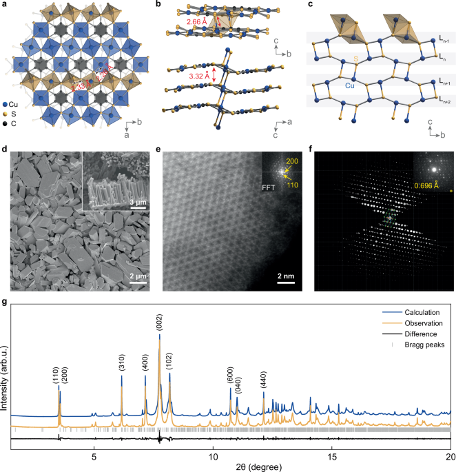
at 75 °C for 1 week, as shown in Supplementary Figs. 1–4. The scanning electron microscopy (SEM) image presented in Fig. 1d illustrates that highly oriented micro-crystal is densely packed
in the Cu3BHT film. These crystals are significantly larger than those reported in previous studies8, with lengths reaching several micrometers and a cross-sectional area exceeding 104 nm2.
Additionally, phase-pure single crystals of Cu3BHT, which are suitable for both the single structure determination and single-crystal device fabrication, can now be efficiently produced
through simple ultrasonication of Cu3BHT micro-crystal arrays. The powder X-ray diffraction (PXRD) patterns and Raman spectra of the synthesized Cu3BHT demonstrate markedly improved quality
over previous studies8,10, particularly with respect to the full width at half maximum (FWHM) and the significantly increased number of detectable peaks (Supplementary Figs. 5–7). These
improvements in crystallinity are crucial for enhancing the resolution of structural determination for Cu3BHT. The synchrotron PXRD (λ = 0.458086 Å) result of the meticulously grown Cu3BHT
samples is displayed in Fig. 1g. The sample’s monoclinic crystal system is well-indexed, with unit cell parameters _a_ = 14.8082(10) Å, _b_ = 8.6706(6) Å, _c_ = 6.8357(5) Å, _α_ = _γ_ = 90°
and _β_ = 97.342(2)°. Notably, two closely spaced peaks at the lowest angle (3.51° and 3.57°, d-spacing = 7.4788 and 7.3531 Å) are indexed as (110) and (200), respectively. These peaks,
corresponding to the in-plane hexagonal periodic packing, were indistinguishable in previous reports due to peak overlap8,10. This finding indicates that the in-plane structure of Cu3BHT
possesses a lower symmetry than a perfect hexagonal lattice. SINGLE CRYSTAL STRUCTURE CHARACTERIZATION OF CU3BHT The successful synthesis of high-quality crystals enabled the first
atomic-resolution structure analysis of Cu3BHT. High-resolution scanning transmission electron microscopy (HR-STEM) images revealed a 2D kagome lattice of Cu atoms in Cu3BHT (Fig. 1e and
Supplementary Fig. 8), which is consistent with previous reports8,10,30. Furthermore, the atomic-precision structure of Cu3BHT was directly solved using the Microcrystal electron diffraction
(Micro-ED) method in TEM with an _ab_ initio approach. As shown in Fig. 1f, the structure of Cu3BHT is depicted along the _c_-axis. The high resolution of the Micro-ED dataset, reaching up
to 0.696 Å (indicated by the yellow circle), facilitated the direct location of all non-hydrogen atoms within the structure (Supplementary Fig. 9). In contrast, previous structure
determinations of Cu3BHT only reached a resolution of 2.3660 Å10. This structure was subsequently refined against high-resolution synchrotron PXRD data through Rietveld refinement. Our
results indicate that Cu3BHT crystallizes in the monoclinic _P_21/_c_ space group, indicating an ABAB double-layer stacking structure. The single crystal structure of Cu3BHT is depicted in
Fig. 1. Each BHT ligand is surrounded by six Cu atoms, with Cu–S distances ranging from 2.26(1) to 2.33(9) Å (Supplementary Fig. 10). Each Cu atom is linked to two BHT ligands, forming a
kagome lattice (Fig. 1a and Supplementary Fig. 11). Notably, the atomic-resolution structure has revealed a critical feature of Cu3BHT that was previously overlooked. Unlike the commonly
assumed van der Waals interactions and _π_–_π_ interactions between layers in 2D c-CPs, Cu–S bonds (2.662(6) Å) are present to connect adjacent Cu3BHT layers (Fig. 1b). The length of the
Cu–S bonds reported here is similar to other Cu–S bonds that have been observed in the crystal structures of other materials35,36. There are two distinct coordination environments for Cu
within Cu3BHT. Specifically, two-thirds of the Cu atoms exhibit 4-coordination in a square planar geometry, whereas the remaining third are 5-coordinated, forming a square pyramidal
structure. Similarly, the S atoms split into two-thirds μ2 and one-third μ3 categories. Although the average interlayer distance is 3.32 Å, a markedly shorter covalent contact of 2.66 Å
occurs between the layers through Cu–S bonds. From another structural perspective, it can be seen as a Cu–S network of the 4.8.8 net, aligned with the (100) plane. The axial Cu–S bonds link
the layers vertically, endowing Cu3BHT with a distinctive non-van der Waals 2D structure that includes both a fully conjugated 2D plane and vertically oriented short covalent interactions
between layers (Fig. 1c). SINGLE CRYSTAL DEVICE CHARACTERIZATION Four probe single-crystal devices were fabricated to reveal the intrinsic electrical properties of Cu3BHT. The SEM image of
the device (Fig. 2a) reveals that a typical Cu3BHT crystal exhibits a rod-like morphology with an edge-on orientation. Four electrodes (5 nm Ti/250 nm Au) were deposited perpendicular to the
long axis of the crystal, enabling the characterization of charge transport along the out-of-plane direction ([001] direction) (Supplementary Figs. 12–14). In Supplementary Fig. 13, the SEM
image and elemental mapping confirm the structural integrity of the Cu3BHT single-crystal device, with no visible cracks or boundary damage observed after electron beam lithography (EBL).
This stability is attributed to the precise optimization of electron beam dosage, ensuring effective photoresist development while preserving the crystal structure. As indicated in Fig. 2b,
the linear voltage-current behavior confirms the Ohmic contact, ensuring the reliability of electrical measurements. The negligible difference in conductivity between two-probe and
four-probe measurements at room temperature confirms minimal contact resistance between Cu3BHT and the electrodes. The electrical conductivity of Cu3BHT along the out-of-plane direction is
estimated to be approximately 103 S/cm at 300 K, increasing to 104 S/cm at 2 K (Fig. 2b, c). The high interlayer conductivity may be attributed to van der Waals and _π–π_ interactions, as
well as the covalently bonded Cu–S network, as shown in the previous discussion (Fig. 1c). The interlayer Cu–S bonding may not only increase the efficiency of charge carrier transport but
also stabilize the stacking structure, preventing the Peierls transition37,38. Figure 2c shows the temperature dependence of normalized out-of-plane resistivity (_ρ_(_T_)/_ρ_(300 K) vs _T_),
with the residual-resistance ratio (RRR) value reaching up to 10, comparable to that of typical copper exposed to environmental conditions39. This is significantly higher than other
metallic MOFs, which typically have RRR values close to 18,10, indicating the high quality of our Cu3BHT crystal and its strong metallic behavior. The temperature-dependent resistivity and
conductivity of the single-crystal devices were characterized using the four-probe method, as illustrated in Supplementary Figs. 15 and 16. Three devices were measured, and their results
were compared with those previously reported poly-crystalline Cu-BHT samples8,10. All three single-crystal devices consistently demonstrated clear metallic behavior from 2 to 300 K. The
measurements based on film samples are more sample-dependent (Supplementary Fig. 17). This is primarily due to the film samples containing numerous crystal boundaries and less precise
control over crystal orientations, resulting in a mixture of intrinsic and extrinsic charge transport properties. In conclusion, our results provide a more intrinsic and detailed picture of
the charge transport properties of Cu3BHT. The log(_ρ_) vs log(_T_) plot in Fig. 2d illustrates that the temperature dependence of Cu3BHT can be divided into three distinct regimes. At very
low temperatures ( < 10 K), the resistivity of Cu3BHT shows minimal temperature dependence, marked by a pronounced minimum resistance value. This phenomenon may be attributed to the
significant exchange coupling between the conduction electron gas and impurities (such as trace amounts of free Cu2+ ions), which induces a novel electronic state that stabilizes the
resistivity. Between 20 and 100 K, the resistivity exhibits a linear temperature dependence, _ρ∝T_, which can be attributed to the metallic charge transport behavior. This linear dependence
is often regarded as a key indicator of non-Fermi-liquid behavior40. As the temperature rises, the amplitude of lattice vibrations escalates, consequently intensifying electron–phonon
scattering. However, as temperatures surpass 100 K, the resistivity exhibits a power-law dependence, _ρ_∝_T_0.31. This change is likely due to the saturation of lattice vibrations and
carrier scattering mechanisms, where the scattering probability ceases to increase significantly with temperature, leading to a slower rise in resistivity. The single-crystal device used in
this study enables the exploration of complex metallic behaviors in 2D c-CPs that were previously unexplored. The metallic properties of Cu3BHT are supported by the results of
magnetoresistance measurements shown in Fig. 2e. When subjected to an external magnetic field at 1.7 K, the electrical resistance of single-crystal Cu3BHT increases by approximately 2%,
consistent with ordinary magnetoresistance41. This response can be attributed to the magnetic field’s effect on electron motion within the lattice, which leads to increased scattering events
and, consequently, higher overall resistance. Additionally, ultraviolet photoelectron spectroscopy (UPS) analysis indicates that the Fermi level of Cu3BHT intersects with the conduction
band, as illustrated in Fig. 2f, providing additional support for the material’s metallic behavior. SUPERCONDUCTIVITY CHARACTERIZATION AND MAGNETIC PROPERTIES To investigate the Cu3BHT
crystal’s magnetic properties, magnetization measurements were performed under applied magnetic fields ranging from 0 to 5 T at various temperatures. The resulting curves consistently
demonstrate paramagnetic characteristics across these temperatures (Fig. 3a). As shown in Fig. 3b, no divergence was observed between the temperature dependence of magnetic susceptibilities
collected from zero-field-cooled (ZFC) and field-cooled (FC) measurements, indicating the absence of long-range magnetic ordering down to at least 2 K. The temperature dependence of magnetic
susceptibility, _χ(T)_, was examined under a 500 mT magnetic field. The inverse susceptibility, _χ_−1(_T_), was also calculated and is presented in Fig. 3c. The susceptibility and its
inverse curve clearly follow Curie’s law, further supporting the non-Fermi liquid behavior42. These magnetic characterizations collectively confirm the paramagnetic nature of Cu3BHT down to
at least 2 K. Moreover, _χT_ at 300 K is approximately 0.125 emu K/mol, corresponding to an effective moment of _μ_eff = 0.577_μ__B_. This value is roughly one-third of the expected value
for Cu2+ ions with _S_ = 1/2 (_μ_eff = 1.73_μ__B_). This suggests that approximately one-third of the Cu atoms in Cu3BHT should be Cu2+. The temperature dependence of the direct current (DC)
magnetic susceptibility for Cu3BHT microcrystals from different batches is in excellent agreement, thereby confirming the reproducibility of their magnetic properties (Supplementary Fig.
18). This conclusion is further supported by _X_-ray photoelectron spectroscopy (XPS) analysis (Supplementary Fig. 19), which indicates that both Cu⁺ and Cu²⁺ exist in Cu3BHT with a ratio of
approximately 2:1. Combined with the crystal structure analysis, it is suggested that Cu²⁺ ions are associated with a square pyramidal structure, while Cu⁺ ions adopt a square planar
coordination geometry. These results also suggest that copper exhibits mixed valence in Cu3BHT, with the total anionic charge of BHT being −4. The mixed valence of copper in Cu3BHT may be
caused by metal-to-ligand charge transfer rather than the involvement of an external oxidizing agent. When Cu²⁺ is reduced to Cu⁺, the ligand is oxidized to a −4 state. Since three
equivalents of Cu²⁺ and one equivalent of BHT6− participate in the reaction, the result is a net zero charge. Even when charge transfer occurs between the copper and the ligand, the result
is a net zero charge. In the Cu3BHT crystal, a sharp decline in resistance is observed as the temperature drops to 0.25 K, signaling the onset of superconductivity. The superconducting
transition is highly abrupt, with a transition width Δ_T_c of 40 mK, which is significantly smaller than the transition temperature (Fig. 3d). Furthermore, additional devices exhibit
superconducting transitions, though with slight variations in transition temperature and Δ_T_c, likely arising from differences in crystal and device quality (Supplementary Fig. 20). The
close agreement in transition temperature between the examined Cu3BHT crystal and the thin film sample suggests that both host the same superconducting phase, further highlighting the
intrinsic characteristics and reproducibility of the material. In the magnetic field range of 0 to 1 T applied along the _ab_ plane and the supercurrent flowing along the _c_-axis, the
superconducting critical temperature (_T_c) shifts toward lower temperatures as the magnetic field strength increases (Fig. 3e). At a magnetic field of 1 T, the superconductivity completely
vanishes. By employing the Werthamer–Helfand–Hohenberg (WHH) formula43, the critical magnetic field at zero temperature for Cu3BHT is determined to be 0.15 T (Fig. 3f), and the
superconducting coherence length is computed as 47 nm using the expression \({{{\upxi }}}_{0}=[{\Phi }_{0}/2{{\uppi }}{{{{\rm{H}}}}}_{c2}{[0]\left. \right)}]^{0.5}\). This relatively large
coherence length is significantly smaller than the sample diameter (~200 nm), indicating the presence of bulk superconductivity. BAND STRUCTURE CALCULATION Density functional theory (DFT)
electronic band structure calculation was conducted based on the atomic-precise crystal structure of Cu3BHT, revealing its inherent metallic properties (Fig. 4a and Supplementary Fig. 21),
which is in good agreement with UPS results. At the Fermi level, notable contributions to the density of state (DOS) stem from the _d_ orbitals of Cu, as well as the _p_ orbitals of S and C
(Supplementary Fig. 22), indicating a pronounced degree of conjugation within the material. The electron band structure of Cu3BHT is depicted along the high-symmetry points of the first
Brillouin zone (Fig. 4b), revealing prominent bands crossing the Fermi level along several directions, including Γ–M, Γ–A, A–M, M–B, Γ–B, and Z–D, indicating its metallic properties within
the plane. Moreover, particular emphasis is placed on the material’s metallic characteristics extending into the _c_ direction, as demonstrated by the band crossings at the Fermi level in
the out-of-plane directions Γ–Z and B–D. The in-plane metallic behavior arises from the conductive pathway of _π_–_d_ conjugation interactions between transition metal _d_ orbitals and
organic ligand _π_ orbitals, with the kagome structure formed by densely connected square pyramidal Cu atoms and BHT ligands. In the _c_ direction, the metallicity predominantly arises from
interlayer Cu–S bonds formed by pentacoordinate Cu atoms and adjacent S atoms, which play a more significant role than van der Waals interactions, significantly enhancing perpendicular
conductivity. The phonon spectrum and density of states for various atoms (Fig. 4c), along with the Eliashberg spectral function and the cumulative frequency function of the electron–phonon
coupling (EPC) strength in Cu3BHT (Fig. 4d), indicate pronounced EPC at frequencies below 6 THz, where phonons are predominantly contributed by the vibrations of Cu and S atoms.
Specifically, the coordination of square pyramidal Cu atoms with S atoms within layers and the coordination of pentacoordinate Cu atoms with S atoms from adjacent layers, play a major role.
The Cu–S bonds not only enhance electron–electron interactions within and between layers but also strengthen electron–phonon coupling, significantly contributing to the material’s
superconducting properties. This underscores the importance of interlayer Cu–S bonding along the _π_–_π_ stacking direction and provides new insights into the out-of-plane structural
characteristics of kagome superconductors. Furthermore, the vibrational coupling between S and C atoms at frequencies around 10 THz indicates strong in-plane EPC, whereas the high-frequency
stretching vibrations of C atoms at frequencies above 30 THz contribute relatively less to the overall EPC strength (Supplementary Fig. 23). By unfolding the electronic band structures to
the Brillouin zone of the kagome lattice formed by Cu atoms within Cu3BHT, characteristic features of a kagome band structure are observed, including the Dirac cone at the corners of the
Brillouin zone, a van Hove singularity at the zone boundary center, and a flat band extending across the entire Brillouin zone (Supplementary Fig. 24). Despite the presence of hybridized
gaps resulting from interactions between the kagome bands and other metallic bands, this exploration has the potential to uncover a wealth of emergent quantum phenomena, which are profoundly
significant for discovering and understanding of new kagome superconductors. The Cu3BHT structure achieves superconductivity through unique mechanisms that enhance both electron–electron
interactions and electron–phonon coupling. This structure features a layered arrangement where organic ligands and metal ions create _π_–_d_ conjugated conductive pathways within an
exceptionally dense kagome lattice. The interlayer connectivity is further augmented by pentadentate Cu atoms, which form Cu–S bonds with S atoms from adjacent layers, thereby shortening
electron transport distances, increasing electron density, and avoiding Peierls distortion. These features significantly amplify electron–electron interactions. The primary contributors to
electron–phonon coupling in Cu3BHT are the Cu and S atoms, along with the plane’s S and C atoms. Interlayer Cu–S bonds further enhance electron–phonon coupling effects in this material. The
unique kagome lattice structure and interlayer Cu–S bonds collectively optimize these properties, distinguishing Cu3BHT’s superconductivity from other organic–inorganic hybrid materials.
DISCUSSION In summary, our study, for the first time, achieved the atomic-precise crystal structure analysis of Cu3BHT, showcasing a unique non-van der Waals 2D structure characterized by
strong interlayer interactions through Cu–S covalent bonds. Single-crystal devices of Cu3BHT oriented in the out-of-plane direction exhibited a complex metallic behavior and a
superconducting transition at 0.25 K. DFT calculations indicate that the covalently bonded intralayer structure enhances electron–electron interactions and electron–phonon coupling,
contributing to the observed properties. These findings deepen the understanding of crystal packing structure and electrical properties of c-CP materials, thus paving the way for the design
of other c-CP-based metallic and superconducting materials. These materials will be anticipated to have a substantial impact on the development of c-CP-based quantum devices. METHODS
MATERIALS CuCl2 was purchased from Alfa Aesar China (Tianjin) Co., Ltd. Toluene was purchased from Beijing Yili Fine Chemicals Co. Ltd. Water was purified using the Milli-Q purification
system. Both solvents were degassed by Freeze–Thaw method before use. Benzenehexathiol (BHT) was synthesized according to the literatures44. All the processing solvents, including ultra-dry
methanol, ultra-dry ethanol, acetone, methyl isobutyl ketone (MIBK), polymethyl methacrylate, and methyl methacrylate, were purchased from commercial sources and used as received. All
commercially available chemicals were used without further purification unless otherwise noted. All air- and water-sensitive reactions were performed under a nitrogen atmosphere. MICRO-ED
DATA COLLECTION AND PROCESSION OF CU3BHT The sample powder was finely pulverized using an agate mortar, then dispersed in pure ethanol and ultrasonicated for 2 min to ensure even
distribution. A small amount of this dispersion was then carefully placed onto a copper grid, which had been prepared with a holey carbon film. The specimen underwent Micro-ED analysis using
a JEOL JEM2100 transmission electron microscope (TEM) operating at 200 kV. This microscope was fitted with a Timepix pixel detector by Amsterdam Scientific Instruments. To reduce the risk
of beam-induced damage, the specimen was cooled to 96 K using a Gatan cryo-transfer tomography holder before the start of data collection. A Cu3BHT crystal was then positioned within the
electron beam and aligned to the correct mechanical eucentric height. Throughout the data collection phase, the goniometer was in constant rotation, capturing selected-area Electron
Diffraction patterns from the crystal at a spot size of 3 with 0.5 s exposure times for each pattern. STRUCTURE DETERMINATION OF CU3BHT The final unit cell parameters were refined using
synchrotron powder X-ray diffraction (SPXRD) through Pawley fitting, which determined the parameters to be _a_ = 14.8082(10) Å, _b_ = 8.6706(6) Å, _c_ = 6.8357(5) Å, with the angles _α_ =
_γ_ = 90° and _β_ = 97.342(2)°. Following this, ab initio structure solution of the merged 3D Electron Diffraction (ED) data was conducted using superflip software. This process successfully
identified all non-hydrogen atoms within the space group _P_21/_c_ for the preliminary structural model. The final structural refinement was carried out using Jana20065, employing the unit
cell parameters obtained from SPXRD. _Powder X-ray Diffraction (PXRD) analyses_ were performed using a Panalytical Rigaku D X-ray powder diffractometer, utilizing Cu Kα radiation (_λ_ =
1.5406 Å) from a D/max 2500 source and Shanghai synchrotron radiation light source (_λ_ = 0.458086 Å). Measurements covered a 2_θ_ range from 5° to 60°, with a step increment of 0.023° and
an exposure duration of 60 s for each step. _Scanning electron microscopy (SEM)_ studies were conducted on an FEI Quattro S instrument, operating across an acceleration voltage range of 5 to
30 kV. Given the excellent conductivity of Cu3BHT, the process did not necessitate any supplementary metal coating. _High-resolution transmission electron microscopy (HRTEM)_ images were
captured using a JEOL 2100F transmission electron microscope at an acceleration voltage of 120 kV. _Cryo-electron microscopy (cryo-EM)_ study was performed on an FEI Titan Krios TEM (Gatan
K2 summit camera) operated at 300 kV with a GIF Quantum energy filter (Gatan). _High-resolution scanning transmission electron microscopy (STEM)_ images were produced with a Nion UltraSTEM
100 microscope, featuring a spherical aberration corrector and an operational voltage of 60 kV. _Ultraviolet photoelectron spectroscopy (UPS) and X-ray photoelectron spectroscopy (XPS)_ were
performed using the Kratos AXIS Ultra Photoelectron Spectrometer. The measurements were conducted under ultra-high vacuum conditions (3 × 10⁻⁹ Torr). The excitation sources used are He I
(21.11 eV) and monochromatic light source Al Kα (1486.6 eV). All binding energy values displayed were calibrated to the C1s peak at 284.8 eV, and data analysis was carried out using the
Avantage software. _Raman spectroscopy_ was conducted using a Horiba spectrometer with 532 nm laser excitation to investigate the structural properties of Cu3BHT. DEVICE FABRICATION
Initially, Cu3BHT was ultrasonically dispersed in methanol, the dispersion was meticulously applied onto a pre-defined Si/SiO2 substrate via a spin-coating process to ensure solvent
evaporation and the uniform distribution of single crystals. Following this, the substrate was coated with MMA and PMMA, which were then subjected to thermal annealing at temperatures of 150
°C and 170 °C for a duration of two minutes, respectively. Utilizing a 30 kV electron beam, lithographic patterning was conducted, with MIBK serving as the developer for the exposed
patterns. This was succeeded by the deposition of a 5 nm titanium layer and a 250 nm gold layer through the process of magnetron sputtering. The fabrication sequence was finalized with a
lift-off process in acetone, culminating in the preparation of the device. _Variable temperature electrical conductivity_ data of single crystals using autocube attoDRY 2100 with SR830
Lock-In Amplifier. Single crystal devices were bonded to chips of attoDRY 2100 with aluminum wire using WestBond 7476D wire bonder. _Magnetic properties_ were assessed using a Quantum Design
Dynacool D-209 Physical Property Measurement System (PPMS). These measurements of susceptibility were conducted in an external field of 500 mT across temperatures from 1.7 to 300 K. The
data were then adjusted to account for the diamagnetic effects, using both measurements from a blank sample holder and Pascal’s constants for correction. _The superconductivity_ measurements
over a temperature range of 0.05 to 1 K were performed using a Quantum Design PPMS DynaCool system equipped with an Electrical Transport Option. In a custom four-contact probe cell, copper
wires were affixed to the sample puck’s copper current collector. _The superconductivity_ of Cu3BHT was estimated based on the calculation of electronic propriety, phonon spectrum, and EPC
strength within the framework of DFT45,46 and density-functional perturbation theory47, which is implemented in the QE package48. The generalized gradient approximation (GGA) in the
functional type of Perdew–Burke–Ernzerh (PBE)49 was employed for the ultrasoft pseudopotentials, and the cutoff energy was set to 80 Ry for wave functions and 640 Ry for charge density.
During structural relaxation and self-consistent calculations, the Gaussian spreading value of 0.01 Ry was employed for the method of Methfessel–Paxton first-order spreading to determine
electron occupations under the uniform 4 × 2 × 4 K-point mesh. The dynamic matrix and phonon frequency were computed on a 1 × 1 × 1 Q-point mesh with a 4 × 2 × 4 K-point sampling in the
Brillouin zone of Cu3BHT, and a finer 8 × 4 × 8 K-point grid is used for the EPC calculations. The cumulative frequency-dependent _λ_(_ω_) was calculated from the Eliashberg spectral
function \({\alpha }^{2}F(\omega )\) via the formula \(\lambda (\omega )=2{\int }_{\!0}^{\omega }d{\omega }^{{\prime} }\frac{{\alpha }^{2}F({\omega }^{{\prime} })}{{\omega }^{{\prime} }}\).
The total EPC _λ_ corresponds to the value of _λ_(_ω_max) with the _ω_max being the maximum of phonon frequency. The superconducting transition temperature was envaulted from the
McMillan–Allen–Dynes (MAD) \({T}_{C}=\frac{{\omega }_{\log }}{1.2}\exp \left[\frac{-1.04\times (1+\lambda )}{\lambda -{\mu }^{*}\times (1+0.62\times \lambda )}\right]\)50,51. Here the
Coulomb pseudopotential \({\mu }^{*}\) is set to 0.1 and the logarithmically averaged frequency \({\omega }_{\log }\) is defined by \({\omega }_{\log }=\exp \left[\frac{2}{\lambda }{\int
}_{\!0}^{\infty }\frac{{\alpha }^{2}F(\omega )}{\omega }{{\mathrm{ln}}}\omega d\omega \right]\). The Vienna Ab initio Simulation Package (VASP)52 was employed to unfolding electronic band
structures to the Brillouin zone of kagome lattice formed by the Cu atoms within Cu3BHT, where the GGA-PBE49 and projector augmented wave pseudopotentials53 with the energy cutoff of 500 eV
were used. DATA AVAILABILITY Crystallographic data for the structures reported in this Article have been deposited at the Cambridge Crystallographic Data Center under deposition number CCDC
12381830. Copies of the data can be obtained free of charge via https://www.ccdc.cam.ac.uk/structures/. The data supporting our findings are included in the article and supplementary files.
Additional data generated during the study are available from the corresponding author upon request. Source data are provided in this paper. REFERENCES * Givaja, G., Amo-Ochoa, P.,
Gómez-García, C. J. & Zamora, F. Electrical conductive coordination polymers. _Chem. Soc. Rev._ 41, 115–147 (2012). Article CAS PubMed Google Scholar * Wang, M. C., Dong, R. H. &
Feng, X. L. Two-dimensional conjugated metal-organic frameworks (2D _c_-MOFs): chemistry and function for MOFtronics. _Chem. Soc. Rev._ 50, 2764–2793 (2021). Article CAS PubMed Google
Scholar * Xie, L. S., Skorupskii, G. & Dinca, M. Electrically conductive metal-organic frameworks. _Chem. Rev._ 120, 8536–8580 (2020). Article CAS PubMed PubMed Central Google
Scholar * Li, H., Eddaoudi, M., O’Keeffe, M. & Yaghi, O. M. Design and synthesis of an exceptionally stable and highly porous metal-organic framework. _Nature_ 402, 276–279 (1999).
Article ADS CAS Google Scholar * Talin, A. A. et al. Tunable electrical conductivity in metal-organic framework thin-film devices. _Science_ 343, 66–69 (2014). Article ADS CAS PubMed
Google Scholar * Dou, J. H. et al. Atomically precise single-crystal structures of electrically conducting 2D metal-organic frameworks. _Nat. Mater._ 20, 222–228 (2021). Article ADS CAS
PubMed Google Scholar * Feng, D. W. et al. Robust and conductive two-dimensional metal-organic frameworks with exceptionally high volumetric and areal capacitance. _Nat. Energy_ 3, 30–36
(2018). Article ADS CAS Google Scholar * Huang, X. et al. A two-dimensional _π-d_ conjugated coordination polymer with extremely high electrical conductivity and ambipolar transport
behaviour. _Nat. Commun._ 6, 7408 (2015). Article ADS CAS PubMed Google Scholar * Huang, X. et al. Highly conducting neutral coordination polymer with infinite two-dimensional
silver-sulfur networks. _J. Am. Chem. Soc._ 140, 15153–15156 (2018). Article CAS PubMed Google Scholar * Huang, X. et al. Superconductivity in a copper(II)-based coordination polymer
with perfect kagome structure. _Angew. Chem. Int. Ed._ 57, 146–150 (2018). Article CAS Google Scholar * Kambe, T. et al. Redox control and high conductivity of nickel bis(dithiolene)
complex π-nanosheet: a potential organic two-dimensional topological insulator. _J. Am. Chem. Soc._ 136, 14357–14360 (2014). Article CAS PubMed Google Scholar * Liu, J. X. et al.
On-liquid-gallium surface synthesis of ultrasmooth thin films of conductive metal-organic frameworks. _Nat. Synth._ 3, 715–726 (2024). Article Google Scholar * Dou, J. H. et al. Signature
of metallic behavior in the metal-organic frameworks M3(hexaiminobenzene)2 (M = Ni, Cu). _J. Am. Chem. Soc._ 139, 13608–13611 (2017). Article CAS PubMed Google Scholar * Park, J. et al.
Stabilization of hexaaminobenzene in a 2D conductive metal-organic framework for high power sodium storage. _J. Am. Chem. Soc._ 140, 10315–10323 (2018). Article CAS PubMed Google Scholar
* Skorupskii, G. et al. Efficient and tunable one-dimensional charge transport in layered lanthanide metal-organic frameworks. _Nat. Chem._ 12, 131–136 (2020). Article CAS PubMed Google
Scholar * Day, R. W. et al. Single crystals of electrically conductive two-dimensional metal-organic frameworks: structural and electrical transport properties. _ACS Cent. Sci._ 5,
1959–1964 (2019). Article CAS PubMed PubMed Central Google Scholar * Hmadeh, M. et al. New porous crystals of extended metal-catecholates. _Chem. Mat._ 24, 3511–3513 (2012). Article
CAS Google Scholar * Sheberla, D. et al. Conductive MOF electrodes for stable supercapacitors with high areal capacitance. _Nat. Mater._ 16, 220–224 (2017). Article ADS CAS PubMed
Google Scholar * Miner, E. M. et al. Electrochemical oxygen reduction catalysed by Ni3(hexaiminotriphenylene)2. _Nat. Commun._ 7, 10942 (2016). Article ADS CAS PubMed PubMed Central
Google Scholar * Sheberla, D. et al. High electrical conductivity in Ni3(2,3,6,7,10,11-hexaiminotriphenylene)2, a semiconducting metal-organic graphene analogue. _J. Am. Chem. Soc._ 136,
8859–8862 (2014). Article CAS PubMed Google Scholar * Dong, R. et al. High-mobility band-like charge transport in a semiconducting two-dimensional metal-organic framework. _Nat. Mater._
17, 1027–1032 (2018). Article ADS CAS PubMed Google Scholar * Banda, H., Dou, J. H., Chen, T. Y., Zhang, Y. G. & Dinca, M. Dual-ion intercalation and high volumetric capacitance in
a two-dimensional non-porous coordination polymer. _Angew. Chem. Int. Ed._ 60, 27119–27125 (2021). Article CAS Google Scholar * Zhu, B. J., Wen, D. S., Liang, Z. B. & Zou, R. Q.
Conductive metal-organic frameworks for electrochemical energy conversion and storage. _Coord. Chem. Rev._ 446, 214119 (2021). Article CAS Google Scholar * Kambe, T. et al. π-Conjugated
nickel bis(dithiolene) complex nanosheet. _J. Am. Chem. Soc._ 135, 2462–2465 (2013). Article CAS PubMed Google Scholar * Zhang, L. Z. et al. Intrinsic two-dimensional organic topological
insulators in metal-dicyanoanthracene lattices. _Nano Lett._ 16, 2072–2075 (2016). Article ADS CAS PubMed Google Scholar * Wang, Z. F., Liu, Z. & Liu, F. Organic topological
insulators in organometallic lattices. _Nat. Commun._ 4, 1471 (2013). Article ADS CAS PubMed Google Scholar * Lin, L. et al. Lattice strained induced spin regulation in Co-N/S
coordination-framework enhanced oxygen reduction reaction. _Angew. Chem. Int. Ed._ 63, 202319518 (2024). Article Google Scholar * Misumi, Y. et al. Quantum spin liquid state in a
two-dimensional semiconductive metal-organic framework. _J. Am. Chem. Soc._ 142, 16513–16517 (2020). Article CAS PubMed Google Scholar * Galeotti, G. et al. Synthesis of mesoscale
ordered two-dimensional π-conjugated polymers with semiconducting properties. _Nat. Mater._ 19, 874–880 (2020). Article ADS CAS PubMed Google Scholar * Takenaka, T. et al. Strongly
correlated superconductivity in a copper-based metal-organic framework with a perfect kagome lattice. _Sci. Adv._ 7, eabf3996 (2021). Article ADS CAS PubMed PubMed Central Google
Scholar * Zhang, X. M., Zhou, Y. N., Cui, B., Zhao, M. W. & Liu, F. Theoretical discovery of a superconducting two-dimensional metal-organic framework. _Nano Lett._ 17, 6166–6170
(2017). Article ADS CAS PubMed Google Scholar * Fan, K., Zhang, C. Y., Chen, Y., Wu, Y. C. & Wang, C. L. The chemical states of conjugated coordination polymers. _Chemistry_ 7,
1224–1243 (2021). Article CAS Google Scholar * Han, J. L. et al. Determining factors in the growth of MOF single crystals unveiled by in situ interface imaging. _Chemistry_ 8, 1637–1657
(2022). Article CAS Google Scholar * Howarth, A. J. et al. Best practices for the synthesis, activation, and characterization of metal-organic frameworks. _Chem. Mat._ 29, 26–39 (2017).
Article ADS CAS Google Scholar * Tang, K. L., Jin, X. L., Long, Y. L., Cui, P. & Tang, Y. Q. Study on the reaction of the anionic copper selenolate complex [Me4N]2[Cu4(SePh)6] with
CS2 in solvents: the crystal structure of a polymeric complex [CuS2COMe]n(I). _J. Chem. Res._ 9, 452–453 (2000). * Valigura, D., Ondrejovic, G. & Kratsmarsmogrovic, J. Space orientation
and bonding properties of thiourea in _N_-salicylideneglycinatocopper(II) complex. _Chem. Pap._ 41, 183–193 (1987). CAS Google Scholar * Radisavljevic, B. & Kis, A. Mobility
engineering and a metal-insulator transition in monolayer MoS2. _Nat. Mater._ 12, 815–820 (2013). Article ADS CAS PubMed Google Scholar * Denoyer, F., Comes, F., Garito, A. F. &
Heeger, A. J. X-ray-diffuse-scattering evidence for a phase transition in tetrathiafulvalene tetracyanoquinodimethane (TTF-TCNQ). _Phys. Rev. Lett._ 35, 445–449 (1975). Article ADS CAS
Google Scholar * Fickett, F. R. Oxygen-free copper at 4K-resistance and magnetoresistance. _IEEE Trans. Magn._ 19, 228–231 (1983). Article ADS Google Scholar * Das, P., Saha, P., Singh,
M., Kumar, P. & Patnaik, S. Quantum linear magnetoresistance and fermi liquid behavior in Kagome Metal Ni3In2S2. Preprint at _arXiv_ https://doi.org/10.48550/arXiv.2402.10096 (2024). *
Ross, A. et al. Structural sensitivity of the spin Hall magnetoresistance in antiferromagnetic thin films. _Phys. Rev. B_ 102, 094415 (2020). Article ADS CAS Google Scholar * Löhneysen,
H. v. et al. Non-Fermi-liquid behavior in a heavy-fermion alloy at a magnetic instability. _Phys. Rev. Lett_. 72, 3262–3265 (1994). * Werthamer, N. R., Helfand, E. & Hohenberg, P. C.
Temperature and purity dependence of the superconducting critical field, _H__c2_. III. electron spin and spin-orbit effects. _Phys. Rev._ 147, 295–302 (1965). * Yip, H. K., Schier, A.,
Riede, J. & Schmidbaur, H. Benzenehexathiol as a template rim for a golden wheel: synthesis and structure of [{CSAu(PPh3)}6]. _J. Chem. Soc. Dalton Trans_. 15, 2333–2334 (1994). *
Hohenberg, P. & Kohn, W. Inhomogeneous electron gas. _Phys. Rev. B_ 136, B864–B871 (1964). Article ADS MathSciNet Google Scholar * Kohn, W. & Sham, L. J. Self-consistent
equations including exchange and correlation effects. _Phys. Rev._ 140, A1133–A1138 (1965). Article ADS MathSciNet Google Scholar * Baroni, S., de Gironcoli, S., Dal Corso, A. &
Giannozzi, P. Phonons and related crystal properties from density-functional perturbation theory. _Rev. Mod. Phys._ 73, 515–562 (2001). Article ADS CAS Google Scholar * Giannozzi, P. et
al. Quantum ESPRESSO toward the exascale. _J. Chem. Phys._ 152, 154105 (2020). Article ADS CAS PubMed Google Scholar * Perdew, J. P., Burke, K. & Ernzerhof, M. Generalized gradient
approximation made simple. _Phys. Rev. Lett._ 78, 1396–1396 (1997). Article ADS CAS Google Scholar * McMillan, W. L. Transition temperature of strong-coupled superconductors. _Phys.
Rev._ 167, 331–344 (1968). Article ADS CAS Google Scholar * Allen, P. B. & Dynes, R. C. Transition temperature of strong-coupled superconductors reanalyzed. _Phys. Rev. B_ 12,
905–922 (1975). Article ADS CAS Google Scholar * Kresse, G. & Furthmuller, J. Efficiency of ab-initio total energy calculations for metals and semiconductors using a plane-wave basis
set. _Comput. Mater. Sci._ 6, 15–50 (1996). Article CAS Google Scholar * Blochl, P. E. Projector augmented-wave method. _Phys. Rev. B_ 50, 17953–17979 (1994). Article ADS CAS Google
Scholar Download references ACKNOWLEDGEMENTS This work was financially supported by the National Key R&D Program of China (Grant No. 2023YFE0206400), the National Natural Science
Foundation of China (Grant No. 22171185, No. 12488201), and the Clinical Medicine Plus X-Young Scholars Project at Peking University, backed by the Fundamental Research Funds for the Central
Universities. The staff of beamlines BL17B1, BL14B1, and BL18U1 of the National Facility for Protein Science Shanghai (NFPS) at the Shanghai Synchrotron Radiation Facility (SSRF) are
acknowledged for their assistance in the data collection. We appreciate the Molecular Materials and Nanofabrication Laboratory (MMNL) in the College of Chemistry and Electron Microscopy
Laboratory of Peking University for the support of instruments to perform device fabrication and characterization. Cryo-EM data were collected on the Electron Microscopy Laboratory of Peking
University with the assistance. Thanks to Ms. Li Xuemei for her help in sample preparation and data collection. X.Z. acknowledges financial support from the National Natural Science
Foundation of China (No. 12004357). Thanks to Dr. Yigang Jin for his help in the powder refinement of the PXRD date of BHT. Thanks to Ze Li, Sha Wu, and Xinyu Wang for conducting the IR and
Raman spectroscopy measurements. S.W. and L.S. acknowledge financial support from the Zhejiang Provincial Natural Science Foundation of China (Grant No. XHD23B0301) and the Research Center
for Industries of the Future (RCIF Project No. WU2023C006) as well as thank Dr. Chao Zhang, Yingchao Wang, and the Instrumentation and Service Center for Material Sciences at Westlake
University for the support with the electrical characterization. We sincerely appreciate Qingqing Ji, Jingyue Wang, and Yue Lu for their helpful discussion. AUTHOR INFORMATION Author notes *
These authors contributed equally: Zhichao Pan, Xing Huang. AUTHORS AND AFFILIATIONS * National Key Laboratory of Advanced Micro and Nano Manufacture Technology, School of Materials Science
and Engineering, Peking University, Beijing, 100871, China Zhichao Pan, Yunlong Fan & Jin-Hu Dou * Key Laboratory of Polymer Chemistry and Physics of Ministry of Education, School of
Materials Science and Engineering, Peking University, Beijing, 100871, China Zhichao Pan, Yunlong Fan & Jin-Hu Dou * Center for Advancing Electronics Dresden & Faculty of Chemistry
and Food Chemistry, Technische Universität Dresden, Dresden, 01062, Germany Xing Huang * Department of Chemistry and Department of Physics, School of Science, Westlake University, Hangzhou,
310030, China Shaoze Wang & Lei Sun * State Key Laboratory of Heavy Oil Processing, College of New Energy and Materials, China University of Petroleum, Beijing, 102249, China Yiyu Liu
& Ying Xing * College of Chemistry and Molecular Engineering, Peking University, Beijing, 100871, China Xuzhong Cong * National Key Laboratory of Advanced Micro and Nano Manufacture
Technology, School of Integrated Circuits, Peking University, Beijing, 100871, China Tingsong Zhang & Yu-Qing Zheng * Beijing Advanced Innovation Center for Integrated Circuits, School
of Integrated Circuits, Peking University, Beijing, 100871, China Tingsong Zhang & Yu-Qing Zheng * International Center for Quantum Materials, School of Physics, Peking University,
Beijing, 100871, China Shichao Qi & Jian Wang * School of Chemistry and Chemical Engineering, Nanjing University, Nanjing, 210093, China Jian Li * College of Physics and Optoelectronic
Engineering, Ocean University of China, Qingdao, Shandong, 266100, China Xiaoming Zhang * Beijing National Laboratory for Molecular Sciences, Key Laboratory of Organic Solids, Institute of
Chemistry Chinese Academy of Sciences, Beijing, 100190, China Wei Xu * Collaborative Innovation Center of Quantum Matter, Beijing, 100871, China Jian Wang Authors * Zhichao Pan View author
publications You can also search for this author inPubMed Google Scholar * Xing Huang View author publications You can also search for this author inPubMed Google Scholar * Yunlong Fan View
author publications You can also search for this author inPubMed Google Scholar * Shaoze Wang View author publications You can also search for this author inPubMed Google Scholar * Yiyu Liu
View author publications You can also search for this author inPubMed Google Scholar * Xuzhong Cong View author publications You can also search for this author inPubMed Google Scholar *
Tingsong Zhang View author publications You can also search for this author inPubMed Google Scholar * Shichao Qi View author publications You can also search for this author inPubMed Google
Scholar * Ying Xing View author publications You can also search for this author inPubMed Google Scholar * Yu-Qing Zheng View author publications You can also search for this author inPubMed
Google Scholar * Jian Li View author publications You can also search for this author inPubMed Google Scholar * Xiaoming Zhang View author publications You can also search for this author
inPubMed Google Scholar * Wei Xu View author publications You can also search for this author inPubMed Google Scholar * Lei Sun View author publications You can also search for this author
inPubMed Google Scholar * Jian Wang View author publications You can also search for this author inPubMed Google Scholar * Jin-Hu Dou View author publications You can also search for this
author inPubMed Google Scholar CONTRIBUTIONS J.D., Z.P., and X.H. conceived the idea and designed the experiments. X.H. synthesized the samples. J.L. and W.X. conducted the structural
analysis. Z.P., Y.F. X.C., and T.Z. performed the material investigations, fabricated single crystal devices, and conducted the electrical measurements. X.Z. performed the DFT calculations
of superconductivity and electronic property. S.W., S.Q., L.S., and J.W. conducted the magnetic and superconductivity performance tests. Y.L. and Y.X. performed the fitting of the
superconducting phase diagram. Z.P., X.H., Y.F., Y.Z., and J.D. analyzed the experimental data and wrote the main manuscript. J.D. supervised the entire project. All authors contributed to
the data analysis and provided feedback on the manuscript. CORRESPONDING AUTHOR Correspondence to Jin-Hu Dou. ETHICS DECLARATIONS COMPETING INTERESTS The authors declare no competing
interests. PEER REVIEW PEER REVIEW INFORMATION _Nature Communications_ thanks Carlos Gómez-García, Hiroshi Nishihara, and Takasada Shibauchi for their contribution to the peer review of this
work. A peer review file is available. ADDITIONAL INFORMATION PUBLISHER’S NOTE Springer Nature remains neutral with regard to jurisdictional claims in published maps and institutional
affiliations. SUPPLEMENTARY INFORMATION SUPPLEMENTARY INFORMATION TRANSPARENT PEER REVIEW FILE SOURCE DATA SOURCE DATA RIGHTS AND PERMISSIONS OPEN ACCESS This article is licensed under a
Creative Commons Attribution-NonCommercial-NoDerivatives 4.0 International License, which permits any non-commercial use, sharing, distribution and reproduction in any medium or format, as
long as you give appropriate credit to the original author(s) and the source, provide a link to the Creative Commons licence, and indicate if you modified the licensed material. You do not
have permission under this licence to share adapted material derived from this article or parts of it. The images or other third party material in this article are included in the article’s
Creative Commons licence, unless indicated otherwise in a credit line to the material. If material is not included in the article’s Creative Commons licence and your intended use is not
permitted by statutory regulation or exceeds the permitted use, you will need to obtain permission directly from the copyright holder. To view a copy of this licence, visit
http://creativecommons.org/licenses/by-nc-nd/4.0/. Reprints and permissions ABOUT THIS ARTICLE CITE THIS ARTICLE Pan, Z., Huang, X., Fan, Y. _et al._ Synthesis and structure of a
non-van-der-Waals two-dimensional coordination polymer with superconductivity. _Nat Commun_ 15, 9342 (2024). https://doi.org/10.1038/s41467-024-53786-1 Download citation * Received: 18 June
2024 * Accepted: 17 October 2024 * Published: 29 October 2024 * DOI: https://doi.org/10.1038/s41467-024-53786-1 SHARE THIS ARTICLE Anyone you share the following link with will be able to
read this content: Get shareable link Sorry, a shareable link is not currently available for this article. Copy to clipboard Provided by the Springer Nature SharedIt content-sharing
initiative