Play all audios:
Download PDF Article Open access Published: 03 January 2025 Rapid cryogenic characterization of 1,024 integrated silicon quantum dot devices Edward J. Thomas ORCID:
orcid.org/0009-0003-0015-66381,2 na1, Virginia N. Ciriano-Tejel ORCID: orcid.org/0000-0001-5185-48211 na1, David F. Wise ORCID: orcid.org/0000-0003-3883-86291, Domenic Prete ORCID:
orcid.org/0000-0002-8044-09241, Mathieu de Kruijf ORCID: orcid.org/0000-0001-5616-43361,3, David J. Ibberson ORCID: orcid.org/0000-0003-3623-44691, Grayson M. Noah ORCID:
orcid.org/0009-0000-1110-12511, Alberto Gomez-Saiz ORCID: orcid.org/0000-0001-5902-02071, M. Fernando Gonzalez-Zalba ORCID: orcid.org/0000-0001-6964-37581, Mark A. I. Johnson ORCID:
orcid.org/0000-0002-5818-01341 & …John J. L. Morton ORCID: orcid.org/0000-0002-0891-11111,2,3 Show authors Nature Electronics volume 8, pages 75–83 (2025)Cite this article
8970 Accesses
1 Citations
28 Altmetric
Metrics details
Subjects Electrical and electronic engineeringElectronic and spintronic devices AbstractAs quantum processors grow in complexity, new challenges arise such as the management of device variability and the interface with supporting electronics. Spin qubits in silicon quantum dots
can potentially address these challenges given their control fidelities and potential for compatibility with large-scale integration. Here we report the integration of 1,024 independent
silicon quantum dot devices with on-chip digital and analogue electronics, all operating below 1 K. A high-frequency analogue multiplexer provides fast access to all devices with minimal
electrical connections, allowing characteristic data across the quantum dot array to be acquired and analysed in under 10 min. This is achieved by leveraging radio-frequency reflectometry
with state-of-the-art signal integrity, characterized by a typical signal-to-noise voltage ratio in excess of 75 for an integration time of 3.18 μs. We extract key quantum dot parameters by
automated machine learning routines to assess quantum dot yield and understand the impact of device design. We find correlations between quantum dot parameters and room-temperature
transistor behaviour that could be used as a proxy for in-line process monitoring.
Similar content being viewed by others Qubits made by advanced semiconductor manufacturing Article Openaccess 29 March 2022 On-demand electrical control of spin qubits Article 12 January 2023 Assessment of the errors of high-fidelity two-qubit gates in silicon quantum dots Article Open
access 20 August 2024 Main
Semiconductor quantum dots (QDs) are a potential platform to implement a fault-tolerant quantum computer, a novel computing paradigm expected to outperform classical high-performance
computers in areas such as materials and drug discovery, database searches and factorization. This is due to their small footprint, ability to host coherent and controllable spin qubits, and
their potential compatibility with advanced semiconductor manufacturing. Spin qubits in isotopically enriched silicon have, in particular, demonstrated control, preparation and read-out
fidelities1,2,3,4,5 above the threshold to perform quantum error correction6. However, such fault tolerance—in which an error-correcting code reduces the error rate to a negligible amount—is
predicted to require millions of physical qubits to resolve practical problems7.
As solid-state quantum processors scale up to useful levels of complexity, two important challenges must be addressed. First, the number of connections between the room-temperature processor
and the quantum processor cannot continue to grow in proportion with the number of qubits8,9,10. Frequency-division multiplexing has been applied to allow multiple qubits to share
measurement electronics. However, frequency crowding limits this approach, so far, to eight qubits per line11. Crossbar approaches12,13, in which \(O(\sqrt{N})\) lines intersect at N qubit
locations, offer an elegant solution to reduce wiring, although with stringent requirements on qubit variability and limitations in processor operation. Ultimately, the use of switches to
achieve time-division multiple access (TDMA), as in dynamic random-access memory, in both read-out and control lines to each qubit unit cell provides the greatest flexibility and
scalability. For d.c. signals, off-chip and on-chip cryogenic switches with ratios up to 1:36 and 1:64, respectively, have been used to address quantum device arrays12,14,15. Multiplexed
control circuitry operating at 1 K with >100 MHz pulsing has also recently been reported16. For radio-frequency (rf) signals used for high-speed read-out, up to 1:3 switching has been shown
on chip17,18,19, and high-frequency 1:4 cryogenic multiplexers (MUXs) have been used with superconducting qubits20. Developing TDMA at scale requires an efficient interface between classical
electronics and the quantum processor.
The second challenge is managing and minimizing process variability between the qubits21, requiring each qubit to be independently characterized and tuned. Minimizing process variability is
already an integral component of modern semiconductor manufacturing. However, current process characterization is optimized for classical transistors, and extending this to quantum devices
requires substantial development in high-throughput cryogenic testing capabilities. State-of-the-art methods rely on newly developed cryogenic probing to enable wafer-scale testing22.
However, this method is currently limited to temperatures above 1.6 K and is unable to efficiently utilize the wafer space since nanometre-scale devices need to be directly contacted to
macroscopic pads. On-chip multiplexing techniques can provide access to large numbers of densely packed devices with minimal input/output connections, whereas testing can be performed under
the optimal temperature conditions of spin qubit devices (millikelvins)12,17. Large-scale on-chip switching of rf signals, therefore, addresses both short-term and long-term challenges in
quantum computer development: providing a way to characterize many quantum devices to address process variability, and to address many qubits in scaled-up quantum processors.
In this Article, we report the rapid characterization of 1,024 QD devices fabricated using a commercial foundry process by integrating high-speed classical multiplexing electronics to
individually address each device. We develop tools to automatically extract key indicators for QD performance and their suitability for use in qubit technologies. We perform a statistical
analysis of different device dimensions, and under varied operating conditions. Ultimately, we show that the electrostatic properties of these devices can be characterized at cryogenic
temperatures in under 10 min of measurement time (Supplementary Section I) by means of rf reflectometry techniques. We also establish a link between cryogenic and room-temperature device
properties, opening a new avenue for pre-cryogenic validation of silicon qubit technologies.
Cryogenic multiplexed access to 1,024 QDsWe use an all-to-all MUX that enables the selection of a single cell given a 10-bit input. It contains an analogue bus of three device control lines and ten digital address lines (five
row-select lines and five column-select lines) to address each QD device under test in a 32 × 32 array. The devices are selectively connected to the analogue bus using complementary
metal–oxide–semiconductor (CMOS) transmission gates integrated within the same silicon as the quantum devices.
The integrated circuit is designed using an ultrathin body and buried oxide fully depleted silicon-on-insulator process. QDs form in the undoped channel of the transistors when a voltage
difference VGS between the gate and source approaches the threshold voltage (Fig. 1b). To observe the discrete charging of QDs, a source and drain tunnelling resistance larger than the
resistance quantum is necessary. This occurs naturally in these devices due to the increase in resistivity of the undoped silicon region at low temperatures. This region lies beneath the
gate and spacers (Fig. 1b). In Fig. 1c, we show an example of the characteristic discrete charging, which is a diamond-shaped region of decreased conductance nestled within regions of higher
conductance.
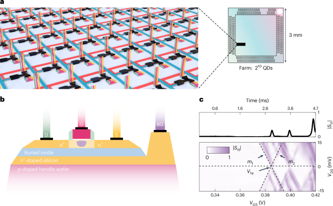
Fig. 1: Measurement of a 1,024 QD farm.a, Schematic of a three-dimensional render of the 1:1,024 MUX, with analogue access (green, VD; pink, VG; yellow, VS) to each QD device controlled by row–column addressing (red and blue
wires). The black bow-tie represents the transmission gates (formed by the parallel combination of matched n- and p-type transistors); and the AND symbol, a two-input binary cell select.
This farm of devices occupies a small section of a 3 mm × 3 mm silicon die. b, Schematic of the cross-section of a single transistor along the direction of current flow, showing a QD
(purple) below the gate and between the drain and source. The region in which the QD forms is undoped silicon. D, drain; S, source; G, gate; BG, back-gate. c, Example of a two-dimensional
map showing a normalized device response, |S11|, (colour scale) as a function of the drain–source and gate–source voltages. The dashed line shows an automated fit to the first measured
Coulomb blockade oscillation. The top panel shows a line cut at VDS = 0 V (indicated by the dotted line), with the time axis aligning with the voltage axis in the bottom panel.
Full sizeimageReflectometry performance via a MUX
To expedite device measurements, we use rf reflectometry23,24,25,26. Reflectometry can detect QD charge transitions with high bandwidth by measuring changes in device impedance. The
typically high device impedance (>100 kΩ) is matched to a 50 Ω line by embedding the integrated circuit in a matching network containing a superconducting spiral inductor (Methods). This
allows us to monitor the reflected voltage as a function of the device impedance.
Here we characterize the performance of this technique in terms of the signal-to-noise ratio (SNR) and bandwidth at a farm level. A peak in the |S11| trace corresponds to the electrochemical
potential of the QD, aligning with the Fermi level of the source or drain. We define the signal as the height of this peak relative to the mean background, and the noise as the standard
deviation of the background signal. In Fig. 2a, we show the SNR2 value of a QD charge transition as a function of integration time τ. Through linear regression assuming a y intercept of
zero, we determine the minimum integration time required to attain an SNR of 1, which amounts to tmin = 556 ± 6 ps. This minimum integration time serves as a benchmark for evaluating the
read-out performance26 and demonstrates that the MUX does not compromise the signal quality. In fact, our apparatus outperforms the state of the art achieved with reflectometry in
single-electron transistors27. Overall, in the TDMA implementation presented here, the integration time is fixed at tint ≈ 11 μs (Supplementary Section I).
Fig. 2: SNR.a, Power SNR as a function of integration time. Data points correspond to the square of the measured SNR (SNR2) at different integration times τ. We fit this with a straight line (solid
black) through the origin. The minimum integration time tmin, where this line crosses SNR = 1, is approximately 0.5 ns. The insets show example Coulomb oscillations, with normalized
amplitudes, measured at the longest integration time tint = 1.6 ms and shortest integration time tint = 3.18 μs (indicated in red). The horizontal axes in the inset are the gate voltage
(VGS) in volts. b, Normalized SNR for nine devices are each shown as faint grey lines, and the heavy black line is the mean response. The green-shaded region is the mean bandwidth over the
selected devices.
Full size imageNext, we test the bandwidth at the farm level by looking at the dependence of SNR with respect to the probe frequency for nine example devices (Fig. 2b). For TDMA, it is critical that the
frequency region of a high signal overlaps for each device in the farm. We demonstrate that this holds, with the average SNR bandwidth (6.4 MHz), defined as the full-width at half-maximum of
the SNR2 signal, which is similar to the resonator bandwidth (9.5 MHz).
Finally, we show how the cryogenic performance of a fully depleted silicon-on-insulator process28,29 is pivotal in creating our low-temperature multiplexing circuit. In particular,
back-gating through the buried oxide enables the compensation of the known transistor threshold voltage increase at low temperatures, which becomes important when delivering high-frequency
signals through the MUX (Fig. 3). In particular, we measure the on resistance Ron of a single transmission gate over a wide back-gate-voltage range (VNW,PW for the n- and p-type field-effect
transistors, NFET and PFET, respectively) and for multiple common-mode drain/source voltages. During these measurements, the NFET gate is held at VDD = 0.8 V and the PFET gate is held at
VSS = 0 V. By applying a forward back-bias (positive for NFET and negative for PFET), we can reduce Ron by more than an order of magnitude for a common-mode voltage VD = VS = 0.4 V (Fig.
3a). We note that the combination of forward back-bias and the large dimensions of the MUX transistors prevents the undesirable occurrence of Coulomb blockade in the transmission gate. The
impact of back-biasing on rf performance is also evident from the quality of the reflectometry signal. Figure 3b shows two Coulomb oscillations as measured in reflectometry as the MUX
back-bias increases. The two oscillations are well resolved when VNW = −VPW > 1.5 V. However, for lower values, a substantial voltage drop occurs at the MUX, shifting the position of the
oscillations. The shift is accompanied by a reduction in SNR, which—along with the unstable signal behaviour—can be linked to the increasing MUX resistance. We highlight that the back-gate
potentials applied to the analogue circuitry are independent of those applied to the QD devices.
Fig. 3: Integrated cryogenic 1:1,024 MUX performance.a, Ron of a single MUX transmission gate with varied analogue back-gates VNW and VPW for the NFET and PFET, respectively. b, Normalized reflected signal from the device as the analogue
back-gates are varied. The MUX reaches a stable configuration when VNW > 1.5 V and VPW < −1.5 V, corresponding to a transmission gate impedance of ~2 kΩ with VDS = 20 mV.
Full sizeimageAnalysis and extraction of QD features at scale
To characterize the QD devices, we develop a method to automatically extract (Methods) the first observed electron loading voltage (V1e), the gate lever arm (αG) that describes the strength
of the electrostatic coupling of the gate electrode to the dot, and the source–drain lever arm difference (αD − αS) to measure the device asymmetry. More specifically, we define V1e as the
gate voltage at which we first detect a Coulomb oscillation at zero VDS, representing the loading of an electron to a QD that may already contain a number of electrons. These parameters are
the ones that can be extracted unambiguously, using the first measured Coulomb blockade oscillation. To extract further electrostatic properties, like the charging energy, further
oscillations are required; however, for many measured devices, the presence of additional QDs cannot be conclusively ruled out. Furthermore, a secondary charge sensor would be required to
verify that we have reached the single-electron regime; therefore, here, instead, we find the distribution of gate voltages corresponding to the first visible transition using our read-out
methods (reflectometry and d.c. transport) to establish the trends and variability between devices. Though we cannot guarantee reaching the single-electron regime, we have identified these
QDs as being in the few-electron regime30 (Supplementary Section II).
As stated above, a single measurement is used to extract all of these parameters automatically, by monitoring the device as VGS and VDS are varied (Methods). A measurement of this kind is
shown in Fig. 1c. In the farm, eight transistor variants were tested with increasing gate lengths (L) of 28 nm, 40 nm, 60 nm and 80 nm and channel widths (W) of 80 nm and 100 nm. Our first
observation shows that not all transistors can provide good QDs (Fig. 4a). For these devices, we, therefore, cannot extract the QD parameters described above, and therefore, they must first
be filtered out. We have trained a convolutional neural network (CNN) to categorize our devices into three categories: clear Coulomb blockade (good), no Coulomb blockade (bad) and multiple
series QDs (multi), which present as non-closing diamonds (Supplementary Section IV provides more information regarding the classification criteria). Each device is manually labelled by two
domain experts and these labels are used to train the CNN (Methods). The proportion of devices that fall into each category as determined by the CNN is shown in Fig. 4b.
Fig. 4: QD yieldand key parameters.
a, Example two-dimensional maps for nine different devices. The labels indicate the quality of Coulomb blockade observed; ‘multi’ refers to signatures of multiple series dots forming in the
device. b, Relative frequency of each device category for different gate lengths L = [28, 40, 60, 80] nm and channel widths W = [80, 100] nm. These data were extracted using the CNN. c–e,
Distributions of automatically extracted gate voltage for the first detected electron transition (c), gate lever arm (d) and drain–source coupling asymmetry (e) for different gate lengths.
In the rf dataset, there are 150 examples at 28 nm gate length and 71 examples at 40 nm gate length. In the d.c. dataset, there are 156 examples at 28 nm gate length and 81 examples at 40 nm
gate length. The features of the box plot are as follows: centre line, median, box edges (25th and 75th percentiles), whiskers, and minimum and maximum of the dataset excluding outliers
more than 1.5× outside the interquartile range.
Full size imageTo automatically extract the parameters, we developed tools to process data acquired through both transport (d.c.) and reflectometry (rf) measurements. Transistor characteristic measurements
are commonly performed in d.c.; thus, the d.c. data presented here serve as a reference for comparison with the rf data, revealing good agreement between both techniques (Fig. 4c–e and
Extended Data Fig. 1). Moreover, increasing the integration time does not result in a substantive change in the extracted parameters (Extended Data Fig. 2). The parameters V1e, αG and αD −
αS can be determined from the pair of intersecting lines in a charge map (Fig. 1c). The intercept gives V1e, and the lever arms can be calculated from the gradients of the two lines
(Methods). For each charge map, we perform a fitting routine that finds the best pair of lines, with higher weight given to V1e at lower voltages, and intercept close to VDS = 0
V.
Variability of industrially fabricated QDsTo assess the inherent process variability, considerable effort was focused on the design stage to suppress the known sources of semiconductor process variability, for example, layout
effects (Methods). Therefore, the variability we measure is primarily inherent to each device under test. As shown in Fig. 4b, in devices with greater gate lengths, multiple dots are
generated, resulting in complex multi-dot structures. On the contrary, devices with shorter gate lengths yield single QDs. However, in most devices, a small gate length leads to an early
transistor turn-on, resulting in ‘bad’ dots. Overall, the device designs with the highest proportion of good QD features have shorter gate lengths, namely, 28 nm and 40 nm. The two channel
widths do not impart notable differences across the farm. The automatically extracted parameters for these good devices are shown in Fig. 4c–e. With decreasing gate length, we see a lower
threshold voltage due to the increasing effect of the electric field produced by the source and drain, a well-known short-channel transistor effect, probably caused by drain-induced barrier
lowering31. The gate lever arm and lever arm asymmetry remain fairly constant, indicating that dots remain well controlled by the gate even at the smallest dimensions.
For the L = 28 nm case, we find the first observed electron voltages (\(\overline{{V}_{{\rm{1e}}}}=387\pm 22\,{\rm{m}}\,{\rm{V}}\)) and the gate lever arms (\(\overline{{\alpha
}_{{\rm{G}}}}=0.741 \pm 0.082\)) are narrowly distributed. We find the standard deviation of V1e (~22 mV) is comparable to the spacing (25 ± 4 mV) between the first and second observed
electron (V2e) loading voltages, measured from a subset of devices in which a second transition is clearly visible. This suggests that the tight requirements for shared voltage control12 are
within reach, but need further reduction. Alternatively, small variations may be compensated with independent voltage trimming of each of the QD back-gates. However, this comes at the cost
of a greater number of control lines per QD. It must be stressed that the overarching challenge with the presented devices is QD quality, which must be addressed before voltage sharing can
be considered. Determining the exact origin of the variability in QD quality is beyond the scope of this work, but we hypothesize that irregularities in electrostatic potential caused by (1)
an elevated number of two-level fluctuators near the Si/SiO2 interface30 and/or (2) gate metal workfunction inhomogeneities32 could be the cause. We note that the large gate lever arm will
be beneficial when implementing gate-based dispersive read-out26.
The mean dot asymmetry \(\overline{{\alpha }_{{\rm{D}}}-{\alpha }_{{\rm{S}}}}=-0.040 \pm 150\) shows that, on average, the QDs are well centred in the channel. We note that since all the
lever arms must add to 1, a large asymmetry places an upper bound on the gate lever arm, that is, αG ≤ 1 − ∣αD − αS∣ (Supplementary Section V). This result highlights an inverse relation
between the asymmetric QD position within the channel and gate control over the QD, emphasizing the importance of QD location being central under the gate. We note that for the devices here,
the QD is placed between two large conducting leads; however, for larger QD arrays, most dots may only have a single lead, or only other dots nearby. In such devices, the importance of the
short-channel effect we see here is lessened. In light of this, our measurements provide a worst-case indication for dot asymmetry under a single gate.
Room-temperature correlations withQD parameters
It would be ideal to determine the QD parameters without needing to cool the device to cryogenic temperatures. For a QD, once the thermal energy kBT becomes much larger than the charging
energy EC = e2/CΣ ≈ 18.5 meV (Methods), transport through the transistor does not exhibit blockade and the device behaves as a simple transistor. However, we gain a new set of parameters
used in the classical modelling of transistors, such as the threshold voltage (Vth).
We next establish a direct link between QD parameters and classical transistor behaviour (Methods), which allows device yield and uniformity to be assessed without requiring expensive and
time-intensive cooling in a dilution refrigerator. Recent work has correlated classical transistor behaviour from room temperature to 4.2 K (ref. 33); here we extend this to the behaviour of
QDs at lower temperatures. We highlight that pre-cryogenic validation can be an invaluable tool in the life cycle of a silicon quantum computer.
We explore the relation between V1e and Vth obtained from devices with the shortest gate length, L = 28 nm, classified as ‘good’. To explore this, we use probabilistic programming, a
technique that offers an insight into both systematic patterns and random fluctuations in the data. We consider a simple linear model of the form
$${V}_{{\rm{1e}}}({V}_{{\rm{th}}})=\alpha{V}_{{\rm{th}}}+\beta +{\mathcal{N}}(0,\,{\sigma }_{{{\rm{V}}}_{1{\rm{e}}}}).$$ (1)
Here α and β are coefficients of the linear model, and \({\mathcal{N}}(0,\,{\sigma }_{{{\rm{V}}}_{1{\rm{e}}}})\) is a normal distribution that represents the intrinsic random fluctuations in
V1e. In this approach, V1e, Vth and the parameters α, β and \({\sigma }_{{{\rm{V}}}_{1{\rm{e}}}}\) are treated as random variables rather than fixed quantities. We express our initial
expectations using prior distributions, which convey our preliminary knowledge about the parameters before any data are collected. For the priors, we opt for normal distributions
(\({\mathcal{N}}\)), as they offer a balanced representation of our initial understanding without being overly restrictive.
Next, we refine these parameter distributions using Hamiltonian Monte Carlo34, aiming to find the best fit to the observed data for V1e. Figure 5a shows the linear fit extracted by averaging
the Hamiltonian Monte Carlo trial results. The extracted slope (\(\overline{\alpha }=1.01\pm 0.02\)) indicates a clear relationship between room-temperature threshold voltage and the first
observed QD electron loading voltage. It is well known that transistor threshold voltages increase at cryogenic temperatures, and this is also apparent in the V1e offset voltage,
\(\overline{\beta }=210\pm 30\,{\rm{m}}\,{\rm{V}}\).
Fig. 5: Correlation of voltage threshold with electron loading.a, V1e, measured at 50 mK, against Vth, measured at room temperature and analysed using Bayesian modelling techniques to extract an underlying linear relationship. The solid black line is
the average of the estimated linear fits and the shaded region shows the 95% confidence interval over possible linear fits (slope and intercept). The dashed lines represent the 95%
confidence interval for V1e accounting for noise. The solid grey line indicates a nominal Vth used to analyse the distribution of V1e in b. b Comparison of the observed distribution of V1e
extracted from the measured data (red) with the predicted posterior distribution (black), showing a standard deviation of approximately σ ≈ 22 mV.
Full size imageThe result from the model is the posterior distribution of V1e. The uncertainty of the posterior distribution (~22 mV) encompasses variations arising from both \(\overline{{V}_{{\rm{th}}}}\)
(\(\overline{{\sigma }_{{{\rm{V}}}_{{\rm{th}}}}}=15\,{\rm{m}}{\rm{V}}\)) and the intrinsic randomness in V1e (\(\overline{{\sigma }_{{{\rm{V}}}_{1{\rm{e}}}}}=16\pm 1\,{\rm{m}}{\rm{V}}\)).
Completely removing variations in the threshold voltage at the foundry level (\({\sigma }_{{{\rm{V}}}_{{\rm{th}}}}=0\)) would consequently decrease the variation in V1e to \({\sigma
}_{{{\rm{V}}}_{1{\rm{e}}}}=16\,{\rm{m}}{\rm{V}}\).
ConclusionsWe have reported testing a device farm of 1,024 QDs based on simple transistor structures. Our approach can, however, be extended to more complex unit cells, such as coupled QD systems—the
basic building block of semiconductor-based quantum computers. Our rf read-out techniques can be leveraged to embed compact dispersive spin qubit read-out with the unit cells of scaled-up QD
architectures35,36. We developed an integrated CMOS three-channel 1:1,024 analogue MUX, but the capabilities of this silicon technology reach further. Foundry-based platforms could, in
particular, allow the co-integration of ultralow power electronic modules such as digital-to-analogue converters, low-noise amplifiers and digital controllers alongside the qubit system.
These technologies have been demonstrated in stand-alone processes37, but tightly integrating all of these modules with semiconductor qubits—and retaining their qualities—remains an open
challenge, especially given the limited cooling power of cryostats and thermal conductivity of silicon at low temperatures. Our observation that cryogenic parameters of silicon QD devices
can be predicted from room-temperature behaviour has implications for the time and resources required to monitor process variations and optimize the design and production of future quantum
devices. Further development of pre-cryogenic methods and analysis tools could allow wider industry engagement and a substantial cost reduction in technology development, particularly if
further correlations can be extracted when complex unit cells are studied.
Methodsd.c. transport measurementWith a small bias of ~ 1 mV, the transport current formed by the tunnelling of electrons one by one through a QD is typically small (~1 pA to 1,000 pA). To record this level of current, we
use a transimpedance amplifier to convert the current to a voltage with a gain of 107 V A−1. To acquire a Coulomb diamond map, a triangular wave with a frequency of 20 Hz was applied to the
gate and the signal is acquired on the rising edge of the slope. Devices were measured with either five or ten averages; a single transport Coulomb diamond measurement takes approximately 15
s or 30 s.
rf reflectometry measurementMeasuring a high-impedance device in reflectometry requires an impedance-transforming circuit (Supplementary Section VI). This allows changes in an otherwise large device impedance to be
measured by a 50 Ω matched meter, for example, resistance changing from 1,000 kΩ to 100 kΩ. The complex impedance of the QD has contributions from the resistance and capacitance of the
tunnel barrier between the source lead and the dot. When the dot and source electrochemical potentials are equal, the Coulomb blockade is lifted and electrons can tunnel elastically through
the barrier. This results in an apparent change in the barrier resistance and capacitance, the latter of which may have both quantum and junction contributions38,39. This impedance change
can be detected at the 50 Ω output as a change in the reflected rf signal near the resonance frequency.
To measure the Coulomb diamond maps, a triangular waveform with a frequency of 203 Hz was applied to the gate. Signal acquisition occurs during the rising edge of the waveform. The frequency
of the triangular waveform is constrained by the RC low-pass filter on the printed circuit board with a cutoff frequency of fc = 16 kHz.
Each Coulomb diamond map comprises 60 distinct traces, covering a range of source–drain voltages (VDS) from –15 mV to 15 mV. The acquisition time required for measuring the 1,024 Coulomb
diamond maps is 2 min 31 s.
The sampling rate used for acquiring these maps is 1 MSa s−1. However, the effective integration time is constrained to 10.68 μs due to limitations imposed by the room-temperature low-pass
filters for the in-phase and quadrature signals (Supplementary Section I).
Coulomb diamond classification using a neural networkWe categorize devices into three groups based on their Coulomb blockade maps (Fig. 4a).
Good: these devices display a clearly defined hourglass shape in their Coulomb blockade map, enabling parameter extraction (Fig. 1c).
Bad: these devices lack observable Coulomb blockade or exhibiting classical transistor turn-on superimposed with Coulomb blockade. This behaviour is probably caused by low resistances of the
tunnelling barriers.
Multi: these devices form several QDs in series, identifiable by overlapping Coulomb diamonds, giving rise to extended regions of blockade.
On the basis of the above criteria, domain experts manually classified the devices. However, the boundaries between categories can be ambiguous, as evidenced by experts agreeing on the
classification approximately 80% of the time for the same dataset. Examples of such ambiguity are faint hourglass shapes mixed with noise or incomplete hourglass shapes.
Although manual classification worked well with the current number of devices (approximately 1,000), the expected increase in device volume calls for an automated solution. To tackle this
challenge with our modest dataset, we applied strategies proven effective in image classification with limited training data. Specifically, we utilize transfer learning by implementing the
well-known ResNet26d architecture, pre-trained on the extensive ImageNet’s database. This approach enables robust performance despite the scale of our dataset40.
Alongside transfer learning, we used data augmentation techniques like image rotation, warping, zooming and changes in saturation. These methods introduce variety into the training data. In
addition, we incorporate mixup, a technique that generates new images by linearly combining pairs of original training images41.
The neural network processes Coulomb blockade data as greyscale images. The dataset was randomly partitioned, with 80% allocated to a training set and 20%, to a test set. To optimize the
training process, we used the one-cycle policy, which dynamically adjusts the learning rate, increasing it to the maximum and then gradually decreasing it42. This dynamic learning rate
schedule helps regulate the training process, accelerates convergence and reduces sensitivity to the hyperparameter of the learning rate, ensuring a more robust and efficient training phase.
In our neural network implementation, we focus on capturing label uncertainty. This is achieved through label smoothing43. In standard binary assignment, like entropy loss, the correct class
receives a probability of 1 and others, 0. On the contrary, label smoothing adjusts the ground-truth labels by assigning a probability slightly less than 1 to the correct class and
distributing the remaining probability uniformly across all classes. This adjustment helps mitigate over-reliance on specific training labels and encourages the model to generalize better
across different classes.
The performance of the CNN is assessed using the confusion matrix (Extended Data Table 1), yielding an accuracy of 88%. This accuracy level is constrained due to the ambiguous boundaries
between different device classes.
To demonstrate that, we evaluated the ChimeraMix architecture, a state-of-the-art approach, which achieved over 96% classification accuracy using labels from a single expert. ChimeraMix
relies on training a generative adversarial network to mix examples of the same class, augmenting the size of the dataset.
Finally, to optimize the neural network further, we suggest a non-binary scoring system for each Coulomb map (for example, using a scale from one to ten). This approach involves training the
network on labels that reflect the collective agreement among multiple human classifiers, which helps mitigate individual biases. Moreover, adopting this method enables the neural network
to better understand the nuances present in edge cases between good, multi and bad dots.
Parameter extraction from Coulomb diamondsMost key parameters that describe a single QD can be obtained from the position and shape of the Coulomb diamond measurements44,45. When measuring the rf response at the drain, the positive
(negative) edges of the Coulomb diamonds appear when the QD electrochemical potential μdot is aligned with the drain (source) electrochemical potential μD (μS). The first observed electron
loading voltage V1e corresponds to the crossing point of the first pair of these edges (nominally at μS = μD = 0 eV).
The gate lever arm αG = CG/CΣ, where CG is the gate capacitance and CΣ is the sum of the dot capacitance to each terminal, represents the coupling strength of the gate to the dot. This
parameter can be calculated as
$${\alpha }_{{\rm{G}}}={\left(\frac{1}{| {m}_{1}| }+\frac{1}{| {m}_{2}| }\right)}^{-1},$$ (2)where m1 and m2 are the positive and negative gradients of the pair of edges that form the first visible hourglass (Fig. 1c).
Moreover, when a voltage bias is applied antisymmetrically (VD = −VS), the relative coupling capacitance of the source (αS = CS/CΣ) and drain (αD = CD/CΣ) can be directly obtained from the
gradient of the Coulomb diamond edges as
$${\alpha }_{{\rm{D}}}-{\alpha }_{{\rm{S}}}=\frac{{m}_{1}+{m}_{2}}{{m}_{1}-{m}_{2}}.$$ (3)This is a measure of the asymmetry of dot formation under the gate.
The full step-by-step process for extracting the dot parameters from Coulomb blockade maps is detailed in Supplementary Section IV, but we provide a succinct summary here. We perform digital
filtering to reduce noise and enhance contrast in the acquired data, and then apply a Canny edge detection algorithm to digitize the charge stability map and identify the edges of the
Coulomb diamonds. We then use a Hough transform to convert the binary image to information about the edges parametrized by their length and angle. We identify good fits to the first visible
Coulomb oscillation with a pair of long line segments, one with a positive slope and the other with a negative one, which intersect near VDS = 0 V.
Room-temperature measurements andcryogenic correlations
We analyse the transport measurements through transistors at room temperature with a source–drain bias of VDS = 50 mV. Vth is determined by extrapolating the ID–VGS curve, between the
maximum transconductance point max(gm) = max(dID/dVGS) and the maximum subthreshold slope point max(SS) = max(log[ID/VGS]) (ref. 46). Vth is the voltage at which this extrapolated line
intersects ID = 0.
To understand the systematic relationship between V1e and Vth and their random variation, we use the probabilistic programming framework NumPyro47. As stated in the main text, we use a model
defined by three random variables: α, β and σ. These variables are initially set with a suitable prior distribution. The posterior distribution is then formed using Hamiltonian Monte
Carlo34 sampling.
Charging energyWe obtain a charge energy of EC = 18.5 ± 3 meV as EC = ∣e∣ΔVGαG, where ∣e∣ ≈ 1.6 × 10⁻¹⁹ C is the elementary charge, αG is the gate lever arm and ΔVG is the difference between the first and
second detected electron (V2e) loading voltages. Some examples of Coulomb diamonds can be found in the main text showing slightly smaller charging energies than the average.
Devicefabrication
The die was fabricated using the GlobalFoundries 22FDX 22 nm fully depleted silicon-on-insulator process. A single die was used for this study.
Experimental setupThe integrated circuit die was glued to a carrier printed circuit board with conducting silver paste. The die is wire bonded (17.5 μm AlSi) to gold-plated copper tracks. The low-frequency
control lines are routed to a connector to attach to a motherboard, which has passive first-order in-line filtering (RC = 10 μs). The reflectometry line is directly routed to an SMP
connector on the carrier printed circuit board.
All the cryogenic measurements were performed in a Bluefors XLD dilution refrigerator, where the device was mounted to the mixing chamber plate operating at 10 mK. When the chip is powered
on, the die temperature was measured as 600 mK using on-chip thermometry48 (value quoted for a nominally identical die). The reason for this elevated temperature is the static power draw of
approximately 4 μW needed for the digital and analogue support electronics.
A QDevil QDAC II was used to supply the d.c. voltages to the QD device terminals, chip supplies and row/column address lines. To sweep the gate voltage, a triangular wave with 50% duty cycle
was supplied by a Keysight 33500B arbitrary waveform generator. The rf reference signal was generated by a Rohde & Schwarz SMB100B. The reflected signal was amplified by a Low Noise Factory
cryogenic amplifier (LNF-LNC0.2_3A s/n 2541z) at 4 K. This signal is then further amplified at room temperature using two Mini-Circuits amplifiers (ZX60-P103LN+ and ZX60-33LNR-S+) before
being separated into its in-phase and quadrature components using a Polyphase microwave quadrature demodulator (AD0540B). These signals are finally amplified and filtered by a Stanford SR560
and then digitized via a Spectrum M4i.4421-x8 digitizer PCIe card.
For d.c. measurements, we used two transimpedance amplifiers (Basel Precision Instruments SP983c, IF3602 junction field-effect transistor) to simultaneously monitor the source (IS) and drain
(ID) currents. The gain of the amplifiers was set to 107 V A−1 with a low-pass filter bandwidth of 1 kHz. For our measurements, we use Isig = (ID − IS)/2 to remove any offsets. During rf
measurements, the transimpedance amplifiers are removed and the source and drain are directly driven with the QDAC II voltage sources mentioned above.
Data availabilityThe data that support the plots within this paper and other findings of this study are available from the corresponding author upon request.
References Xue, X. et al. Quantum logic with spin qubits crossing the surface code threshold. Nature 601, 343–347 (2022).
Article MATH Google Scholar
Noiri, A. et al. Fast universal quantum gate above the fault-tolerance threshold in silicon. Nature 601, 338 (2022).
Article MATH Google Scholar
Mills, A. R. et al. Two-qubit silicon quantum processor with operation fidelity exceeding 99%. Sci. Adv. 8, eabn5130 (2022).
Article Google Scholar
Yoneda, J. et al. Quantum non-demolition readout of an electron spin in silicon. Nat. Commun. 11, 1144 (2020).
Blumoff, J. Z. et al. Fast and high-fidelity state preparation and measurement in triple-quantum-dot spin qubits. PRX Quantum 3, 010352 (2022).
Article Google Scholar
Fowler, A. G., Mariantoni, M., Martinis, J. M. & Cleland, A. N. Surface codes: towards practical large-scale quantum computation. Phys. Rev. A 86, 032324 (2012).
Article Google Scholar
Beverland, M. E. et al. Assessing requirements to scale to practical quantum advantage. Preprint at https://arxiv.org/abs/2211.07629 (2022).
Gonzalez-Zalba, M. F., Barraud, S., Ferguson, A. J. & Betz, A. C. Probing the limits of gate-based charge sensing. Nat. Commun. 6, 6084 (2015).
Article MATH Google Scholar
Franke, D., Clarke, J., Vandersypen, L. & Veldhorst, M. Rent’s rule and extensibility in quantum computing. Microprocess. Microsyst. 67, 1 (2019).
Article MATH Google Scholar
Vandersypen, L. M. K. et al. Interfacing spin qubits in quantum dots and donors—hot, dense, and coherent. npj Quantum Inf. 3, 34 (2017).
Article Google Scholar
George, R. E. et al. Multiplexing superconducting qubit circuit for single microwave photon generation. J. Low Temp. Phys. 189, 60 (2017).
Article MATH Google Scholar
Bavdaz, P. L. et al. A quantum dot crossbar with sublinear scaling of interconnects at cryogenic temperature. npj Quantum Inf. 8, 86 (2022).
Article Google Scholar
Li, R. et al. A crossbar network for silicon quantum dot qubits. Sci. Adv. 4, eaar3960 (2018).
Article Google Scholar
Al-Taie, H. et al. Cryogenic on-chip multiplexer for the study of quantum transport in 256 split-gate devices. Appl. Phys. Lett. 102, 243102 (2013).
Article MATH Google Scholar
Puddy, R. K. et al. Multiplexed charge-locking device for large arrays of quantum devices. Appl. Phys. Lett. 107, 143501 (2015).
Article Google Scholar
Jadot, B. et al. A cryogenic active router for qubit array biasing from d.c. to 320 MHz at 100 nm gate pitch. In ESSCIRC 2023- IEEE 49th European Solid State Circuits Conference (ESSCIRC)
157–160 (IEEE, 2023).
Ruffino, A. et al. A cryo-CMOS chip that integrates silicon quantum dots and multiplexed dispersive readout electronics. Nat. Electron. 5, 53 (2022).
Article MATH Google Scholar
Schaal, S. et al. A CMOS dynamic random access architecture for radio-frequency readout of quantum devices. Nat. Electron. 2, 236 (2019).
Article MATH Google Scholar
Ward, D. R., Savage, D. E., Lagally, M. G., Coppersmith, S. N. & Eriksson, M. A. Integration of on-chip field-effect transistor switches with dopantless Si/SiGe quantum dots for
high-throughput testing. Appl. Phys. Lett. 102, 213107 (2013).
Article Google Scholar
Acharya, R. et al. Suppressing quantum errors by scaling a surface code logical qubit. Nature 614, 676 (2023).
Article MATH Google Scholar
Gonzalez-Zalba, M. F. et al. Scaling silicon-based quantum computing using CMOS technology. Nat. Electron. 4, 872 (2021).
Article MATH Google Scholar
Neyens, S. et al. Probing single electrons across 300-mm spin qubit wafers. Nature 629, 80–85 (2024).
Article Google Scholar
Schoelkopf, R. J., Wahlgren, P., Kozhevnikov, A. A., Delsing, P. & Prober, D. E. The radio-frequency single-electron transistor (RF-SET): a fast and ultrasensitive electrometer. Science 280,
1238–1242 (1998).
Duty, T. et al. Observation of quantum capacitance in the Cooper-Pair transistor. Phys. Rev. Lett. 95, 206807 (2005).
Article MATH Google Scholar
Wallraff, A. et al. Strong coupling of a single photon to a superconducting qubit using circuit quantum electrodynamics. Nature 431, 162 (2004).
Article MATH Google Scholar
Vigneau, F. et al. Probing quantum devices with radio-frequency reflectometry. Appl. Phys. Rev. 10, 021305 (2023).
Keith, D. et al. Single-shot spin readout in semiconductors near the shot-noise sensitivity limit. Phys. Rev. X 9, 041003 (2019).
MATH Google Scholar
Beckers, A. et al. Characterization and modeling of 28-nm FDSOI CMOS technology down to cryogenic temperatures. Solid-State Electron. 159, 106 (2019).
Article MATH Google Scholar
Cardoso Paz, B. et al. Performance and low-frequency noise of 22-nm FDSOI down to 4.2 K for cryogenic applications. IEEE Trans. Electron Devices 67, 4563 (2020).
Article MATH Google Scholar
de Kruijf, M., Noah, G. M., Gomez-Saiz, A., Morton, J. J. & Gonzalez-Zalba, M. Measurement of cryoelectronics heating using a local quantum dot thermometer in silicon. Chip 3, 100097 (2024).
Troutman, R. & Fortino, A. Simple model for threshold voltage in a short-channel IGFET. IEEE Trans. Electron Devices 24, 1266 (1977).
Article MATH Google Scholar
Zeng, Z., Triozon, F. & Niquet, Y.-M. Carrier scattering by workfunction fluctuations and interface dipoles in high-K/metal gate stacks. In 2016 International Conference on Simulation of
Semiconductor Processes and Devices (SISPAD) 369–372 (IEEE, 2016).
Paz, B. C. et al. Integrated variability measurements of 28 nm FDSOI MOSFETs down to 4.2 K for cryogenic CMOS applications. In 2020 IEEE 33rd International Conference on Microelectronic Test
Structures (ICMTS) 1–5 (IEEE, 2020).
Hoffman, M. D. & Gelman, A. The no-U-turn sampler: adaptively setting path lengths in Hamiltonian Monte Carlo. J. Mach. Learn. Res. 15, 1593–1623 (2014).
Veldhorst, M., Eenink, H. G. J., Yang, C. H. & Dzurak, A. S. Silicon CMOS architecture for a spin-based quantum computer. Nat. Commun. 8, 1766 (2017).
Article Google Scholar
Oakes, G. A. et al. Fast high-fidelity single-shot readout of spins in silicon using a single-electron box. Phys. Rev. X 13, 011023 (2023).
MATH Google Scholar
Xue, X. et al. CMOS-based cryogenic control of silicon quantum circuits. Nature 593, 205 (2021).
Article MATH Google Scholar
Luryi, S. Quantum capacitance devices. Appl. Phys. Lett. 52, 501 (1988).
Article Google Scholar
Büttiker, M., Thomas, H. & Prêtre, A. Mesoscopic capacitors. Phys. Lett. A 180, 364 (1993).
Article MATH Google Scholar
Yosinski, J., Clune, J., Bengio, Y. & Lipson, H. How transferable are features in deep neural networks? Adv. Neural Inf. Process. Syst. 27, 3320–3328 (2014).
MATH Google Scholar
Zhang, H., Cisse, M., Dauphin, Y. N. & Lopez-Paz, D. mixup: beyond empirical risk minimization. Preprint at https://arxiv.org/abs/1710.09412 (2017).
Smith, L. N. & Topin, N. Super-convergence: very fast training of neural networks using large learning rates. In Artificial Intelligence and Machine Learning for Multi-Domain Operations
Applications 1100612 (SPIE, 2019).
Müller, R., Kornblith, S. & Hinton, G. E. When does label smoothing help? Adv. Neural Inf. Process. Syst. 32, 4694–4703 (2019).
MATH Google Scholar
Hanson, R., Kouwenhoven, L. P., Petta, J. R., Tarucha, S. & Vandersypen, L. M. K. Spins in few-electron quantum dots. Rev. Mod. Phys. 79, 1217 (2007).
Article Google Scholar
Yang, T. Y. et al. Quantum transport in 40-nm MOSFETs at deep-cryogenic temperatures. IEEE Electron Device Lett. 41, 981 (2020).
MATH Google Scholar
Pierre, M. et al. Single-donor ionization energies in a nanoscale CMOS channel. Nat. Nanotechnol. 5, 133 (2010).
Article MATH Google Scholar
Phan, D., Pradhan, N. & Jankowiak, M. Composable effects for flexible and accelerated probabilistic programming in NumPyro. Preprint at https://arxiv.org/abs/1912.11554 (2019).
Noah, G. M. et al. CMOS on-chip thermometry at deep cryogenic temperatures. Appl. Phys. Rev. 11, 021414 (2024).
Article MATH Google Scholar
Download references
AcknowledgementsE.J.T. acknowledges the Engineering and Physical Sciences Research Council (EPSRC) through the Centre for Doctoral Training in Delivering Quantum Technologies (grant no. EP/S021582/1).
M.F.G.-Z. acknowledges a UKRI Future Leaders Fellowship (grant no. MR/V023284/1). We thank N. Cave at GlobalFoundries for helpful discussions.
Author informationAuthor notesThese authors contributed equally: Edward J. Thomas, Virginia N. Ciriano-Tejel.
Authors and Affiliations Quantum Motion, London, UK
Edward J. Thomas, Virginia N. Ciriano-Tejel, David F. Wise, Domenic Prete, Mathieu de Kruijf, David J. Ibberson, Grayson M. Noah, Alberto Gomez-Saiz, M. Fernando Gonzalez-Zalba, Mark A. I.
Johnson & John J. L. Morton
Department of Electronic and Electrical Engineering, UCL, London, UK
Edward J. Thomas & John J. L. Morton
London Centre for Nanotechnology, UCL, London, UK
Mathieu de Kruijf & John J. L. Morton
AuthorsEdward J. ThomasView author publications You can also search for this author inPubMed Google Scholar
Virginia N. Ciriano-TejelView author publications You can also search for this author inPubMed Google Scholar
David F. WiseView author publications You can also search for this author inPubMed Google Scholar
Domenic PreteView author publications You can also search for this author inPubMed Google Scholar
Mathieu de KruijfView author publications You can also search for this author inPubMed Google Scholar
David J. IbbersonView author publications You can also search for this author inPubMed Google Scholar
Grayson M. NoahView author publications You can also search for this author inPubMed Google Scholar
Alberto Gomez-SaizView author publications You can also search for this author inPubMed Google Scholar
M. Fernando Gonzalez-ZalbaView author publications You can also search for this author inPubMed Google Scholar
Mark A. I. JohnsonView author publications You can also search for this author inPubMed Google Scholar
John J. L. MortonView author publications You can also search for this author inPubMed Google Scholar
ContributionsE.J.T., V.N.C.-T. and D.P. performed the experiments under the supervision of M.A.I.J. and M.F.G.-Z. M.d.K. and D.J.I. contributed to the preparation of the experiment and preliminary
characterization. M.F.G.-Z. and J.J.L.M. conceived the experiment. A.G.-S. designed the device with contributions from M.F.G.-Z. and J.J.L.M. The device analogue components were validated by
G.M.N. D.F.W. and V.N.C.-T. designed and developed the automated analysis tools. Further data analysis was performed by E.J.T., V.N.C.-T., D.F.W. and M.A.I.J. The manuscript was prepared by
M.A.I.J., V.N.C.-T., D.F.W. and M.F.G.-Z., with contributions from all authors.
Corresponding author Correspondence to Mark A. I. Johnson.
Ethics declarations Competing interestsThe authors declare no competing interests.
Peer review Peer review informationNature Electronics thanks the anonymous reviewers for their contribution to the peer review of this work.
Additional informationPublisher’s note Springer Nature remains neutral with regard to jurisdictional claims in published maps and institutional affiliations.
Extended dataExtended Data Fig. 1 Parametervariation with back-gate voltage.
a-c, Estimated distributions of first observed electron loading voltage, gate lever arm and QD asymmetry as back-gate voltage is varied (L = 28 nm). As backgate increases the dc and rf
datasets have 206, 207, 178, 170, 175 and 176 data points. The box plot features are as follows: centre line, median, box edges 25th and 75th percentile, whiskers, minimum and maximum of the
dataset excluding outliers more than 1.5 × outside the interquartile range.
Extended Data Fig. 2 Parameter extraction performance with increasing integration time.a-c, Distributions of extracted parameters (first detected electron loading voltage, gate lever arm, and source-drain asymmetry) using swarm plots (left) and a box plot (right), as the
number of averages is varied in rf measurements. The swarm plot reveals individual data points’ distribution, while the box plot displays central tendencies and quartiles for easy comparison
and outlier detection. As expected, we observe a decrease in the parameter standard deviation as averages increase. Each group contains 206 samples after removing outliers which are more
than 1.5 × outside the interquartile range. The box plot features are as follows: centre line, median, box edges 25th and 75th percentile, whiskers, minimum and maximum of the dataset
excluding outliers more than 1.5x outside the interquartile range.
Extended Data Table 1 Confusion matrix of the convolutional neural network on the test data setFull sizetableSupplementary informationSupplementary Information
Supplementary Sections I–IX, Figs. 1–7 and Discussion.
Rights and permissionsOpen Access This article is licensed under a Creative Commons Attribution 4.0 International License, which permits use, sharing, adaptation, distribution and reproduction in any medium or
format, as long as you give appropriate credit to the original author(s) and the source, provide a link to the Creative Commons licence, and indicate if changes were made. The images or
other third party material in this article are included in the article’s Creative Commons licence, unless indicated otherwise in a credit line to the material. If material is not included in
the article’s Creative Commons licence and your intended use is not permitted by statutory regulation or exceeds the permitted use, you will need to obtain permission directly from the
copyright holder. To view a copy of this licence, visit http://creativecommons.org/licenses/by/4.0/.
Reprints and permissions
About this articleCite this article Thomas, E.J., Ciriano-Tejel, V.N., Wise, D.F. et al. Rapid cryogenic characterization of 1,024 integrated silicon quantum dot devices. Nat Electron 8,
75–83 (2025). https://doi.org/10.1038/s41928-024-01304-y
Download citation
Received: 13 February 2024
Accepted: 05 November 2024
Published: 03 January 2025
Issue Date: January 2025
DOI: https://doi.org/10.1038/s41928-024-01304-y
Share this article Anyone you share the following link with will be able to read this content:
Get shareable link Sorry, a shareable link is not currently available for this article.
Copy to clipboard Provided by the Springer Nature SharedIt content-sharing initiative