Play all audios:
ABSTRACT The development of an electronic skin is critical to the realization of artificial intelligence that comes into direct contact with humans, and to biomedical applications such as
prosthetic skin. To mimic the tactile sensing properties of natural skin, large arrays of pixel pressure sensors on a flexible and stretchable substrate are required. We demonstrate
flexible, capacitive pressure sensors with unprecedented sensitivity and very short response times that can be inexpensively fabricated over large areas by microstructuring of thin films of
the biocompatible elastomer polydimethylsiloxane. The pressure sensitivity of the microstructured films far surpassed that exhibited by unstructured elastomeric films of similar thickness,
and is tunable by using different microstructures. The microstructured films were integrated into organic field-effect transistors as the dielectric layer, forming a new type of active
sensor device with similarly excellent sensitivity and response times. Access through your institution Buy or subscribe This is a preview of subscription content, access via your institution
ACCESS OPTIONS Access through your institution Subscribe to this journal Receive 12 print issues and online access $259.00 per year only $21.58 per issue Learn more Buy this article *
Purchase on SpringerLink * Instant access to full article PDF Buy now Prices may be subject to local taxes which are calculated during checkout ADDITIONAL ACCESS OPTIONS: * Log in * Learn
about institutional subscriptions * Read our FAQs * Contact customer support SIMILAR CONTENT BEING VIEWED BY OTHERS ULTRAFAST PIEZOCAPACITIVE SOFT PRESSURE SENSORS WITH OVER 10 KHZ BANDWIDTH
VIA BONDED MICROSTRUCTURED INTERFACES Article Open access 08 April 2024 HIGH-SPEED AND LARGE-SCALE INTRINSICALLY STRETCHABLE INTEGRATED CIRCUITS Article 13 March 2024 A FLEXIBLE PRESSURE
SENSOR WITH HIGHLY CUSTOMIZABLE SENSITIVITY AND LINEARITY VIA POSITIVE DESIGN OF MICROHIERARCHICAL STRUCTURES WITH A HYPERELASTIC MODEL Article Open access 04 January 2023 REFERENCES *
Someya, T. et al. Conformable, flexible, large-area networks of pressure and thermal sensors with organic transistor active matrixes. _Proc. Natl Acad. Sci._ 102, 12321–12325 (2005). Article
CAS Google Scholar * Sekitani, T. et al. A rubberlike stretchable active matrix using elastic conductors. _Science_ 321, 1468–1472 (2008). Article CAS Google Scholar * Wagner, S. et
al. Electronic skin: Architecture and components. _Physica E_ 25, 326–334 (2004). Article Google Scholar * Sun, Y., Choi, W. M., Jiang, H., Huang, Y. Y. & Rogers, J. A. Controlled
buckling of semiconductor nanoribbons for stretchable electronics. _Nature Nanotech._ 1, 201–207 (2006). CAS Google Scholar * Dellon, E. S., Mourey, R. & Dellon, A. L. Human pressure
perception values for constant and moving one- and two-point discrimination. _J. Plast. Reconstr. Surg._ 90, 112–117 (1992). Article CAS Google Scholar * Bao, Z. & Locklin, J.
_Organic Field-Effect Transistors_ (CRC Press, 2007). Book Google Scholar * Roberts, M. E. et al. Water-stable organic transistors and their application in chemical and biological sensors.
_Proc. Natl Acad. Sci._ 105, 12134–12139 (2008). Article CAS Google Scholar * Someya, T. et al. A large-area, flexible pressure sensor matrix with organic field-effect transistors for
artificial skin applications. _Proc. Natl Acad. Sci._ 101, 9966–9970 (2004). Article CAS Google Scholar * Voorthuyzen, J. A., Bergveld, P. & Sprenkels, A. J. Semiconductor-based
electret sensors for sound and pressure. _IEEE Trans. Electr. Insul._ 24, 267–276 (1989). Article CAS Google Scholar * Olthuis, W. Chemical and physical FET-based sensors or variations on
an equation. _Sens. Actuat. B_ 105, 96–103 (2005). Article CAS Google Scholar * Hussain, M., Choa, Y-H. & Niihara, K. Conductive rubber materials for pressure sensors. _J. Mater.
Sci. Lett._ 20, 525–527 (2001). Article CAS Google Scholar * Shimojo, M., Namiki, A., Ishikawa, M., Makino, R. & Mabuchi, K. A tactile sensor sheet using pressure conductive rubber
with electrical-wires stitched method. _IEEE Sensors J._ 4, 589–596 (2004). Article Google Scholar * Engel, J., Chen, J., Chen, N., Pandya, S. & Liu, C. _19th International Conference
on MEMS, Istanbul, Turkey_ (IEEE, 2006). Google Scholar * Lee, H-K., Chang, S-I. & Yoon, E. A flexible polymer tactile sensor: Fabrication and modular expandability for large area
deployment. _J. Microelectromech. Syst._ 15, 1681–1686 (2006). Article CAS Google Scholar * Metzger, C. et al. Flexible-foam-based capacitive sensor arrays for object detection at low
cost. _Appl. Phys. Lett._ 92, 013506 (2008). Article Google Scholar * Lee, I. & Sung, H. J. Development of an array of pressure sensors with PVDF film. _Exp. Fluids_ 26, 27–35 (1999).
Article CAS Google Scholar * Shirinov, A. V. & Schomburg, W. K. Pressure sensor from a PVDF film. _Sens. Actuat. A_ 142, 48–55 (2008). Article CAS Google Scholar * Graz, I. et al.
Flexible ferroelectret field-effect transistor for large-area sensor skins and microphones. _Appl. Phys. Lett._ 89, 073501 (2006). Article Google Scholar * Graz, I. et al. Flexible
active-matrix cells with selectively poled bifunctional polymer–ceramic nanocomposite for pressure and temperature sensing skin. _J. Appl. Phys._ 106, 034503 (2009). Article Google Scholar
* Darlinski, G. et al. Mechanical force sensors using organic thin-film transistors. _J. Appl. Phys._ 97, 093708 (2005). Article Google Scholar * Manunza, I., Sulis, A. & Bonfiglio,
A. Pressure sensing by flexible, organic, field effect transistors. _Appl. Phys. Lett._ 89, 143502 (2006). Article Google Scholar * Chan, Y., Mi, Y., Trau, D., Huang, P. & Chen, E.
Micromolding of PDMS scaffolds and microwells for tissue culture and cell patterning: A new method of microfabrication by the self-assembled micropatterns of diblock copolymer micelles.
_Polymer_ 47, 5124–5130 (2006). Article Google Scholar * Balaban, N. Q. et al. Force and focal adhesion assembly: A close relationship studied using elastic micropatterned substrates.
_Nature Cell Biol._ 3, 466–472 (2001). Article CAS Google Scholar * Reese, C., Chung, W-J., Ling, M-M., Roberts, M. E. & Bao, Z. High-performance microscale single-crystal transistors
by lithography on an elastomer dielectric. _Appl. Phys. Lett._ 89, 202108 (2006). Article Google Scholar * Sundar, V. C. et al. Elastomeric transistor stamps: Reversible probing of charge
transport in organic crystals. _Science_ 303, 1644–1646 (2004). Article CAS Google Scholar * Kloc, Ch., Simpkins, P. G., Siegrist, T. & Laudise, R. A. Physical vapour growth of
centimetre-sized crystals of alpha-hexathiophene. _J. Cryst. Growth_ 182, 416–427 (1997). Article CAS Google Scholar * Reese, C. & Bao, Z. Organic single-crystal field-effect
transistors. _Mater. Today_ 10, 20–27 (2007). Article CAS Google Scholar Download references ACKNOWLEDGEMENTS The authors thank J. Locklin for discussions. We thank N. Sutardja and J.
Opatkiewicz for help during the development of the microstructuring technology and the first sensor prototypes. This project was partially funded by NSF ECCS 0730710 and MURI Office of Naval
Research (N000140810654). We thank the Center for Polymer Interface Macromolecular Assemblies (CPIMA) for the use of shared facilities. We also acknowledge the use of the Stanford
Nanocharacterization Laboratory and the Stanford Nanofabrication Facility, partially supported by the National Science Foundation through the National Nanotechnology Infrastructure Network.
Part of this work was done at the Stanford Synchrotron Radiation Laboratory (SSRL), operated by the Department of Energy. S.C.B.M. acknowledges postdoctoral fellowship support by the
Deutsche Forschungsgemeinschaft (DFG) grant MA ∼3342/1-1. B.C-K.T. acknowledges support from a National Science Scholarship from the Agency for Science, Technology and Research (A*STAR),
Singapore. R.M.S. acknowledges support from a National Science Foundation Graduate Fellowship. Z.B. acknowledges support from a Sloan Research Fellowship. AUTHOR INFORMATION AUTHORS AND
AFFILIATIONS * Department of Chemical Engineering, Stanford University, Stanford, California 94305, USA Stefan C. B. Mannsfeld, Christopher V. H-H. Chen, Soumendra Barman, Beinn V. O. Muir,
Anatoliy N. Sokolov, Colin Reese & Zhenan Bao * Department of Electrical Engineering, Stanford University, Stanford, California 94305, USA Benjamin C-K. Tee * Department of Chemistry,
Stanford University, Stanford, California 94305, USA Randall M. Stoltenberg Authors * Stefan C. B. Mannsfeld View author publications You can also search for this author inPubMed Google
Scholar * Benjamin C-K. Tee View author publications You can also search for this author inPubMed Google Scholar * Randall M. Stoltenberg View author publications You can also search for
this author inPubMed Google Scholar * Christopher V. H-H. Chen View author publications You can also search for this author inPubMed Google Scholar * Soumendra Barman View author
publications You can also search for this author inPubMed Google Scholar * Beinn V. O. Muir View author publications You can also search for this author inPubMed Google Scholar * Anatoliy N.
Sokolov View author publications You can also search for this author inPubMed Google Scholar * Colin Reese View author publications You can also search for this author inPubMed Google
Scholar * Zhenan Bao View author publications You can also search for this author inPubMed Google Scholar CONTRIBUTIONS Z.B. and S.C.B.M. conceptualized and directed the research project.
S.C.B.M. developed the first working sensor prototypes. B.C-K.T. developed large portions of the experimental set-ups. S.C.B.M and B.C-K.T. discussed and carried out the majority of the
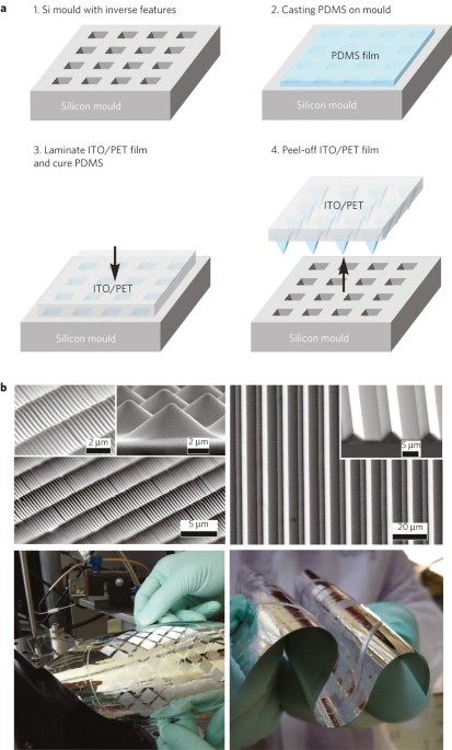
experiments. B.C-K.T. and C.V.H-H.C designed and fabricated the matrix sensor. B.C-K.T. carried out the temperature drift and loading/unloading stability experiments. R.M.S. took the SEM
data. S.B. helped with some experiments. R.M.S., B.C-K.T. and B.V.O.M fabricated the Si moulds. B.V.O.M. fabricated the photolithographic mask. A.N.S. and B.C-K.T carried out most of the
bending-stability experiments. C.R. and B.C-K.T. grew the rubrene crystals. S.C.B.M. wrote the first draft of the manuscript. All authors discussed the results and commented on the
manuscript. CORRESPONDING AUTHOR Correspondence to Zhenan Bao. ETHICS DECLARATIONS COMPETING INTERESTS A patent application is in the process of being filed. No patent was initiated prior to
and at the time of the submission of the paper. SUPPLEMENTARY INFORMATION SUPPLEMENTARY INFORMATION Supplementary Information (PDF 417 kb) RIGHTS AND PERMISSIONS Reprints and permissions
ABOUT THIS ARTICLE CITE THIS ARTICLE Mannsfeld, S., Tee, BK., Stoltenberg, R. _et al._ Highly sensitive flexible pressure sensors with microstructured rubber dielectric layers. _Nature
Mater_ 9, 859–864 (2010). https://doi.org/10.1038/nmat2834 Download citation * Received: 15 March 2010 * Accepted: 16 July 2010 * Published: 12 September 2010 * Issue Date: October 2010 *
DOI: https://doi.org/10.1038/nmat2834 SHARE THIS ARTICLE Anyone you share the following link with will be able to read this content: Get shareable link Sorry, a shareable link is not
currently available for this article. Copy to clipboard Provided by the Springer Nature SharedIt content-sharing initiative