Play all audios:
ABSTRACT Silicon-based transistors are approaching their physical limits and thus new high-mobility semiconductors are sought to replace silicon in the microelectronics industry. Both bulk
materials (such as silicon-germanium and III–V semiconductors) and low-dimensional nanomaterials (such as one-dimensional carbon nanotubes and two-dimensional transition metal
dichalcogenides) have been explored, but, unlike silicon, which uses silicon dioxide (SiO2) as its gate dielectric, these materials suffer from the absence of a high-quality native oxide as
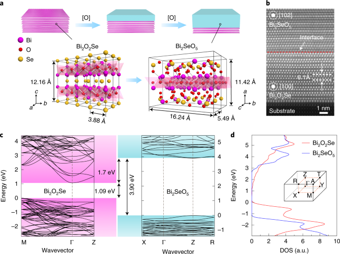
a dielectric counterpart. This can lead to compatibility problems in practical devices. Here, we show that an atomically thin gate dielectric of bismuth selenite (Bi2SeO5) can be conformally
formed via layer-by-layer oxidization of an underlying high-mobility two-dimensional semiconductor, Bi2O2Se. Using this native oxide dielectric, high-performance Bi2O2Se field-effect
transistors can be created, as well as inverter circuits that exhibit a large voltage gain (as high as 150). The high dielectric constant (~21) of Bi2SeO5 allows its equivalent oxide
thickness to be reduced to 0.9 nm while maintaining a gate leakage lower than thermal SiO2. The Bi2SeO5 can also be selectively etched away by a wet chemical method that leaves the mobility
of the underlying Bi2O2Se semiconductor almost unchanged. Access through your institution Buy or subscribe This is a preview of subscription content, access via your institution ACCESS
OPTIONS Access through your institution Access Nature and 54 other Nature Portfolio journals Get Nature+, our best-value online-access subscription $32.99 / 30 days cancel any time Learn
more Subscribe to this journal Receive 12 digital issues and online access to articles $119.00 per year only $9.92 per issue Learn more Buy this article * Purchase on SpringerLink * Instant
access to full article PDF Buy now Prices may be subject to local taxes which are calculated during checkout ADDITIONAL ACCESS OPTIONS: * Log in * Learn about institutional subscriptions *
Read our FAQs * Contact customer support SIMILAR CONTENT BEING VIEWED BY OTHERS A SINGLE-CRYSTALLINE NATIVE DIELECTRIC FOR TWO-DIMENSIONAL SEMICONDUCTORS WITH AN EQUIVALENT OXIDE THICKNESS
BELOW 0.5 NM Article 15 September 2022 SINGLE-CRYSTALLINE VAN DER WAALS LAYERED DIELECTRIC WITH HIGH DIELECTRIC CONSTANT Article 09 March 2023 SCALABLE INTEGRATION OF HYBRID HIGH-_Κ_
DIELECTRIC MATERIALS ON TWO-DIMENSIONAL SEMICONDUCTORS Article 03 August 2023 DATA AVAILABILITY The data that support the plots within this paper and other findings of this study are
available from the corresponding author upon reasonable request. REFERENCES * Kilby, J. S. Invention of the integrated circuit. _IEEE Trans. Electron. Dev._ 23, 648–654 (1976). Article
Google Scholar * Kingon, A. I., Maria, J. P. & Streiffer, S. K. Alternative dielectrics to silicon dioxide for memory and logic devices. _Nature_ 406, 1032–1038 (2000). Article Google
Scholar * Muller, D. A. et al. The electronic structure at the atomic scale of ultrathin gate oxides. _Nature_ 399, 758–761 (1999). Article Google Scholar * Van Zant, P. _Microchip
Fabrication_: _A Practical Guide to Semiconductor Processing_ 4th edn, 100–121 (McGraw Hill, 2000). * Ferain, I., Colinge, C. A. & Colinge, J. P. Multigate transistors as the future of
classical metal–oxide–semiconductor field-effect transistors. _Nature_ 479, 310–316 (2011). Article Google Scholar * Aberg, I., Chleirigh, C. N., Olubuyide, O. O., Duan, X. & Hoyt, J.
L. High electron and hole mobility enhancements in thin-body strained Si/strained SiGe/strained Si heterostructures on insulator. In _Technical Digest of the IEEE International Electron
Devices Meeting 2004_ 173–176 (IEEE, 2004). * Xiang, J. et al. Ge/Si nanowire heterostructures as high-performance field-effect transistors. _Nature_ 441, 489–493 (2006). Article Google
Scholar * Passlack, M. et al. High mobility III–V MOSFETs for RF and digital applications. In _Proceedings of the International Electron Devices Meeting 2007_ 621–624 (IEEE, 2007). *
Ohtomo, A. & Hwang, H. Y. A high-mobility electron gas at the LaAlO3/SrTiO3 heterointerface. _Nature_ 427, 423–426 (2004). Article Google Scholar * Qiu, C. G. et al. Scaling carbon
nanotube complementary transistors to 5-nm gate lengths. _Science_ 355, 271–276 (2017). Article Google Scholar * Shulaker, M. M. et al. Carbon nanotube computer. _Nature_ 501, 526–530
(2013). Article Google Scholar * Desai, S. B. et al. MoS2 transistors with 1-nanometer gate lengths. _Science_ 354, 99–102 (2016). Article Google Scholar * Li, L. K. et al. Black
phosphorus field-effect transistors. _Nat. Nanotechnol._ 9, 372–377 (2014). Article Google Scholar * Bandurin, D. A. et al. High electron mobility, quantum Hall effect and anomalous
optical response in atomically thin InSe. _Nat. Nanotechnol._ 12, 223–227 (2017). Article Google Scholar * Novoselov, K. S. et al. A roadmap for graphene. _Nature_ 490, 192–200 (2012).
Article Google Scholar * Chhowalla, M., Jena, D. & Zhang, H. Two-dimensional semiconductors for transistors. _Nat. Rev. Mater._ 1, 16052 (2016). Article Google Scholar * Franklin, A.
D. Nanomaterials in transistors: from high-performance to thin-film applications. _Science_ 349, aab2750 (2015). Article Google Scholar * Li, M. Y., Su, S. K., Wong, H. S. P. & Li, L.
J. How 2D semiconductors could extend Moore’s law. _Nature_ 567, 169–170 (2019). Article Google Scholar * Liu, Y., Duan, X. D., Huang, Y. & Duan, X. F. Two-dimensional transistors
beyond graphene and TMDCs. _Chem. Soc. Rev._ 47, 6388–6409 (2018). Article Google Scholar * Zhao, H. et al. Effects of gate-first and gate-last process on interface quality of
In0.53Ga0.47As metal–oxide–semiconductor capacitors using atomic-layer-deposited Al2O3 and HfO2 oxides. _Appl. Phys. Lett._ 95, 253501 (2009). Article Google Scholar * Gutowski, M. et al.
Thermodynamic stability of high-_κ_ dielectric metal oxides ZrO2 and HfO2 in contact with Si and SiO2. _Appl. Phys. Lett._ 80, 1897–1899 (2002). Article Google Scholar * Maiti, C. K.,
Samanta, S. K., Chatterjee, S., Dalapati, G. K. & Bera, L. K. Gate dielectrics on strained Si/SiGe heterolayers. _Solid State Electron._ 48, 1369–1389 (2004). Article Google Scholar *
Toriumi, A. et al. Opportunities and challenges for Ge CMOS—control of interfacing field on Ge is a key. _Microelectron. Eng._ 86, 1571–1576 (2009). Article Google Scholar * Hussey, R. J.
et al. Thermal oxidation of III–V materials and heterostructures. _J. Electrochem. Soc._ 149, G581–G584 (2002). Article Google Scholar * Zhu, H. et al. Remote plasma oxidation and atomic
layer etching of MoS2. _ACS Appl. Mater. Interfaces_ 8, 19119–19126 (2016). Article Google Scholar * Chamlagain, B. et al. Thermally oxidized 2D TaS2 as a high-_κ_ gate dielectric for MoS2
field-effect transistors. _2D Mater._ 4, 031002 (2017). Article Google Scholar * Lai, S. et al. HfO2/HfSe2 hybrid heterostructure fabricated via controllable chemical conversion of
two-dimensional HfS2. _Nanoscale_ 10, 18758–18766 (2018). Article Google Scholar * Yamamoto, M. et al. Self-limiting layer-by-layer oxidation of atomically thin WSe2. _Nano Lett._ 15,
2067–2073 (2015). Article Google Scholar * Mleczko, M. J. et al. HfSe2 and ZrSe2: two-dimensional semiconductors with native high-k oxides. _Sci. Adv._ 3, e1700481 (2017). Article Google
Scholar * Peimyoo, N. et al. Laser-writable high-_κ_ dielectric for van der Waals nanoelectronics. _Sci. Adv._ 5, eaau0906 (2019). Article Google Scholar * Wu, J. X. et al. High electron
mobility and quantum oscillations in non-encapsulated ultrathin semiconducting Bi2O2Se. _Nat. Nanotechnol._ 12, 530–535 (2017). Article Google Scholar * Chen, C. et al. Electronic
structures and unusually robust bandgap in an ultrahigh-mobility layered oxide semiconductor, Bi2O2Se. _Sci. Adv._ 4, eaat8355 (2018). Article Google Scholar * Wu, D. et al.
Thickness-dependent dielectric constant of few-layer In2Se3 nanoflakes. _Nano Lett._ 15, 8136–8140 (2015). Article Google Scholar * Lin, Z. et al. Solution-processable 2D semiconductors
for high-performance large-area electronics. _Nature_ 562, 254–258 (2018). Article Google Scholar * Chen, B. et al. Highly uniform carbon nanotube field-effect transistors and medium scale
integrated circuits. _Nano Lett._ 16, 5120–5128 (2016). Article Google Scholar * Tan, C. W. et al. Wafer-scale growth of single-crystal 2D semiconductor on perovskite oxides for
high-performance transistors. _Nano Lett._ 19, 2148–2153 (2019). Article Google Scholar * Kresse, G. & Hafner, J. Norm-conserving and ultrasoft pseudopotentials for first-row and
transition-elements. _J. Phys. Condens. Matter_ 6, 8245–8257 (1994). Article Google Scholar * Heyd, J., Scuseria, G. E. & Ernzerhof, M. Hybrid functionals based on a screened Coulomb
potential. _J. Chem. Phys._ 118, 8207–8215 (2003). Article Google Scholar * Vydrov, O. A., Heyd, J., Krukau, A. V. & Scuseria, G. E. Importance of short-range versus long-range
Hartree–Fock exchange for the performance of hybrid density functionals. _J. Chem. Phys._ 125, 074106 (2006). Article Google Scholar * Wu, X. et al. Quantitative measurements of nanoscale
permittivity and conductivity using tuningfork-based microwave impedance microscopy. _Rev. Sci. Instrum._ 89, 043704 (2018). Article Google Scholar * Wu, J. X. et al. Chemical patterning
of high-mobility semiconducting 2D Bi2O2Se crystals for integrated optoelectronic devices. _Adv. Mater._ 29, 1704060 (2017). Article Google Scholar Download references ACKNOWLEDGEMENTS We
thank G.F. Dong for her help and discussions in measuring dielectric properties. We acknowledge financial support from the National Natural Science Foundation of China (21733001, 21525310,
51672007 and 11974023) and the National Basic Research Program of China (2016YFA0200101). P.G. also acknowledges support from the Key Area R&D Program of Guangdong Province
(2018B010109009) and the Key R&D Program of Guangdong Province (2018B030327001). J.Y. and K.L. were supported by the US Department of Energy (DOE), Office of Science, Basic Energy
Sciences (award no. DE-SC0019025). AUTHOR INFORMATION Author notes * These authors contributed equally: Tianran Li, Teng Tu. AUTHORS AND AFFILIATIONS * Center for Nanochemistry, Beijing
Science and Engineering Center for Nanocarbons, Beijing National Laboratory for Molecular Sciences, College of Chemistry and Molecular Engineering, Peking University, Beijing, China Tianran
Li, Teng Tu, Jinxiong Wu, Yan Liang, Yichi Zhang, Congcong Zhang, Yumin Dai & Hailin Peng * Electron Microscopy Laboratory, School of Physics and International Center for Quantum
Materials, Peking University, Beijing, China Yuanwei Sun & Peng Gao * Department of Condensed Matter Physics, Weizmann Institute of Science, Rehovot, Israel Huixia Fu & Binghai Yan *
Department of Physics, University of Texas at Austin, Austin, TX, USA Jia Yu & Keji Lai * Key Laboratory of Organic Optoelectronics and Molecular Engineering of the Ministry of
Education, Department of Chemistry, Tsinghua University, Beijing, China Lei Xing, Ziang Wang & Liying Jiao * Key Laboratory of Microelectronic Devices and Circuits, Institute of
Microelectronics, Peking University, Beijing, China Huimin Wang, Rundong Jia, Ming Li & Ru Huang * Tianjin Key Lab for Rare Earth Materials and Applications, Center for Rare Earth and
Inorganic Functional Materials, School of Materials Science and Engineering, National Institute for Advanced Materials, Nankai University, Tianjin, China Jinxiong Wu * Academy for Advanced
Interdisciplinary Studies, Peking University, Beijing, China Congwei Tan * Key Laboratory for the Physics and Chemistry of Nanodevices and Department of Electronics, Peking University,
Beijing, China Chenguang Qiu * Collaborative Innovation Centre of Quantum Matter, Beijing, China Peng Gao Authors * Tianran Li View author publications You can also search for this author
inPubMed Google Scholar * Teng Tu View author publications You can also search for this author inPubMed Google Scholar * Yuanwei Sun View author publications You can also search for this
author inPubMed Google Scholar * Huixia Fu View author publications You can also search for this author inPubMed Google Scholar * Jia Yu View author publications You can also search for this
author inPubMed Google Scholar * Lei Xing View author publications You can also search for this author inPubMed Google Scholar * Ziang Wang View author publications You can also search for
this author inPubMed Google Scholar * Huimin Wang View author publications You can also search for this author inPubMed Google Scholar * Rundong Jia View author publications You can also
search for this author inPubMed Google Scholar * Jinxiong Wu View author publications You can also search for this author inPubMed Google Scholar * Congwei Tan View author publications You
can also search for this author inPubMed Google Scholar * Yan Liang View author publications You can also search for this author inPubMed Google Scholar * Yichi Zhang View author
publications You can also search for this author inPubMed Google Scholar * Congcong Zhang View author publications You can also search for this author inPubMed Google Scholar * Yumin Dai
View author publications You can also search for this author inPubMed Google Scholar * Chenguang Qiu View author publications You can also search for this author inPubMed Google Scholar *
Ming Li View author publications You can also search for this author inPubMed Google Scholar * Ru Huang View author publications You can also search for this author inPubMed Google Scholar *
Liying Jiao View author publications You can also search for this author inPubMed Google Scholar * Keji Lai View author publications You can also search for this author inPubMed Google
Scholar * Binghai Yan View author publications You can also search for this author inPubMed Google Scholar * Peng Gao View author publications You can also search for this author inPubMed
Google Scholar * Hailin Peng View author publications You can also search for this author inPubMed Google Scholar CONTRIBUTIONS H.P. conceived the original idea for the project. T.T. carried
out the synthesis and structural characterizations of the bulk and 2D crystals. The devices were fabricated and measured by T.L., with help from L.X., Z.W., H.W. and R.J. H.F. and B.Y.
carried out the theoretical calculations. The scanning transmission electron microscopy measurements were performed by Y.S. under the direction of P.G. MIM was performed by J.Y. under the
supervision of K.L. The manuscript was written by H.P., T.L., T.T. and J.W. with input from the other authors. All work was supervised by H.P. All authors contributed to the scientific
planning and discussions. CORRESPONDING AUTHOR Correspondence to Hailin Peng. ETHICS DECLARATIONS COMPETING INTERESTS The authors declare no competing interests. ADDITIONAL INFORMATION
PUBLISHER’S NOTE Springer Nature remains neutral with regard to jurisdictional claims in published maps and institutional affiliations. SUPPLEMENTARY INFORMATION SUPPLEMENTARY INFORMATION
Supplementary Figs. 1–19. RIGHTS AND PERMISSIONS Reprints and permissions ABOUT THIS ARTICLE CITE THIS ARTICLE Li, T., Tu, T., Sun, Y. _et al._ A native oxide high-_κ_ gate dielectric for
two-dimensional electronics. _Nat Electron_ 3, 473–478 (2020). https://doi.org/10.1038/s41928-020-0444-6 Download citation * Received: 08 October 2019 * Accepted: 22 June 2020 * Published:
27 July 2020 * Issue Date: August 2020 * DOI: https://doi.org/10.1038/s41928-020-0444-6 SHARE THIS ARTICLE Anyone you share the following link with will be able to read this content: Get
shareable link Sorry, a shareable link is not currently available for this article. Copy to clipboard Provided by the Springer Nature SharedIt content-sharing initiative