Play all audios:
ABSTRACT Sensors that are capable of three-dimensional detection of depth field information in the spatial domain are of potential use in applications such as robotics, satellite imaging and
medical assistance. However, current techniques require a precise light source for complex phase detection and diffraction, or involve static multidirectional reflection imaging. Here we
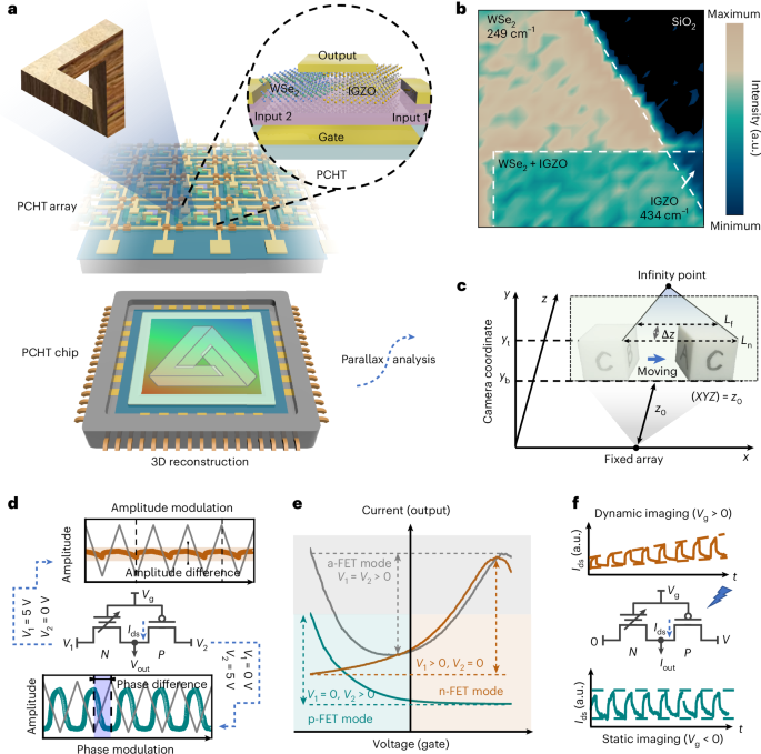
report a reconfigurable heterostructure transistor array for monocular three-dimensional parallax reconstruction. The phototransistors are based on heterostructures of indium gallium zinc
oxide and tungsten diselenide, and can operate as n-type, p-type or ambipolar transistors depending on electrostatic modulation. The arrays can be switched between two modes: a real-time
constant perception mode for static imaging and a spatiotemporal planar configuration mode with memory for dynamic imaging. To switch between the modes, the dominant carrier polarity is
changed via a complementary metal–oxide–semiconductor-compatible multiterminal addressing architecture. We show that the system can be used for three-dimensional morphology reconstruction,
two-dimensional depth field mapping and multi-view coupling. Access through your institution Buy or subscribe This is a preview of subscription content, access via your institution ACCESS
OPTIONS Access through your institution Access Nature and 54 other Nature Portfolio journals Get Nature+, our best-value online-access subscription $29.99 / 30 days cancel any time Learn
more Subscribe to this journal Receive 12 digital issues and online access to articles $119.00 per year only $9.92 per issue Learn more Buy this article * Purchase on SpringerLink * Instant
access to full article PDF Buy now Prices may be subject to local taxes which are calculated during checkout ADDITIONAL ACCESS OPTIONS: * Log in * Learn about institutional subscriptions *
Read our FAQs * Contact customer support SIMILAR CONTENT BEING VIEWED BY OTHERS A UNIVERSAL 3D IMAGING SENSOR ON A SILICON PHOTONICS PLATFORM Article 10 February 2021 HOLOBRICKS: MODULAR
COARSE INTEGRAL HOLOGRAPHIC DISPLAYS Article Open access 16 March 2022 PARALLELIZING ANALOG IN-SENSOR VISUAL PROCESSING WITH ARRAYS OF GATE-TUNABLE SILICON PHOTODETECTORS Article Open access
21 May 2025 DATA AVAILABILITY The data that support the findings of this study are available via Figshare at https://doi.org/10.6084/m9.figshare.26764015 (ref. 41). Source data are provided
with this paper. CODE AVAILABILITY The code used for image reconstruction is available from the corresponding author on reasonable request. REFERENCES * Wu, J. et al. An integrated imaging
sensor for aberration-corrected 3D photography. _Nature_ 612, 62–71 (2022). Article MATH Google Scholar * Lien, M. et al. Ranging and light field imaging with transparent photodetectors.
_Nat. Photonics_ 14, 143–148 (2020). Article MATH Google Scholar * Feng, X., Ma, Y. & Gao, L. Compact light field photography towards versatile three-dimensional vision. _Nat.
Commun._ 13, 3333 (2022). Article MATH Google Scholar * Jing, X. et al. Single-shot 3D imaging with point cloud projection based on metadevice. _Nat. Commun._ 13, 7842 (2022). Article
MATH Google Scholar * Huang, L. et al. Three-dimensional optical holography using a plasmonic metasurface. _Nat. Commun._ 4, 2808 (2013). Article MATH Google Scholar * Park, J., Lee, K.
& Park, Y. Ultrathin wide-angle large-area digital 3D holographic display using a non-periodic photon sieve. _Nat. Commun._ 10, 1304 (2019). Article MATH Google Scholar * Vamvakeros,
A. et al. 5D operando tomographic diffraction imaging of a catalyst bed. _Nat. Commun._ 9, 4751 (2018). Article MATH Google Scholar * Li, J. et al. Rapid sensing of hidden objects and
defects using a single-pixel diffractive terahertz sensor. _Nat. Commun._ 14, 6791 (2023). Article MATH Google Scholar * Cherukara, M. J. et al. Three-dimensional X-ray diffraction
imaging of dislocations in polycrystalline metals under tensile loading. _Nat. Commun._ 9, 3776 (2018). Article MATH Google Scholar * Yi, L., Hou, B., Zhao, H. & Liu, X.
X-ray-to-visible light-field detection through pixelated colour conversion. _Nature_ 618, 281–286 (2023). Article MATH Google Scholar * Shen, Z. et al. Monocular metasurface camera for
passive single-shot 4D imaging. _Nat. Commun._ 14, 1035 (2023). Article MATH Google Scholar * Huang, X. et al. Polarization structured light 3D depth image sensor for scenes with
reflective surfaces. _Nat. Commun._ 14, 6855 (2023). Article MATH Google Scholar * Fang, J., Huang, K., Wu, E., Yan, M. & Zeng, H. Mid-infrared single-photon 3D imaging. _Light Sci.
Appl._ 12, 144 (2023). Article Google Scholar * Zhang, X., Kwon, K., Henriksson, J., Luo, J. & Wu, M. C. A large-scale microelectromechanical systems-based silicon photonics LiDAR.
_Nature_ 603, 253–258 (2022). Article MATH Google Scholar * Rogers, C. et al. A universal 3D imaging sensor on a silicon photonics platform. _Nature_ 590, 256–261 (2021). Article MATH
Google Scholar * Goossens, S. et al. Broadband image sensor array based on graphene-CMOS integration. _Nat. Photonics_ 11, 366–371 (2017). Article MATH Google Scholar * Zhang, Z. A
flexible new technique for camera calibration. _IEEE T. Pattern. Anal._ 22, 1330–1334 (2000). Article MATH Google Scholar * Tachella, J. et al. Real-time 3D reconstruction from
single-photon lidar data using plug-and-play point cloud denoisers. _Nat. Commun._ 10, 4984 (2019). Article MATH Google Scholar * Zhou, K. et al. Parallelized computational 3D video
microscopy of freely moving organisms at multiple gigapixels per second. _Nat. Photon._ 17, 442–450 (2023). Article MATH Google Scholar * Siavashani, M. et al. 3D imaging using scanning
diffractometry. _Sci. Rep._ 11, 482 (2021). Article MATH Google Scholar * Scholler, J. et al. Dynamic full-field optical coherence tomography: 3D live-imaging of retinal organoids. _Light
Sci. Appl._ 9, 140 (2020). Article Google Scholar * Ozyesil, O., Voroninski, V., Basri, R. & Singer, A. A survey of structure from motion. _Acta Numer._ 26, 305–364 (2017). Article
MathSciNet MATH Google Scholar * Schonberger, J. L. & Frahm, J. Structure-from-motion revisited. In _Proc. IEEE Conference on Computer Vision and Pattern Recognition (CVPR)_ 4104–4113
(IEEE, 2016). * Mennel, L. et al. Ultrafast machine vision with 2D material neural network image sensors. _Nature_ 579, 62–66 (2020). Article Google Scholar * Lee, J. et al. Thin-film
image sensors with a pinned photodiode structure. _Nat. Electron._ 6, 590–598 (2023). Article MATH Google Scholar * Pan, C. et al. Reconfigurable logic and neuromorphic circuits based on
electrically tunable two-dimensional homojunctions. _Nat. Electron._ 3, 383–390 (2020). Article Google Scholar * Choi, H. et al. A steep switching WSe2 impact ionization field-effect
transistor. _Nat. Commun._ 13, 6076 (2022). Article MATH Google Scholar * Seyler, K. L. et al. Electrical control of second-harmonic generation in a WSe2 monolayer transistor. _Nat.
Nanotechnol._ 10, 407–411 (2015). Article MATH Google Scholar * Pudasaini, P. R. et al. High-performance multilayer WSe2 field-effect transistors with carrier type control. _Nano Res._
11, 722–730 (2018). Article MATH Google Scholar * Cong, X. et al. Interplay of valley polarized dark trion and dark exciton-polaron in monolayer WSe2. _Nat. Commun._ 14, 5657 (2023).
Article MATH Google Scholar * Ren, Y. et al. Recent advances in ambipolar transistors for functional applications. _Adv. Funct. Mater._ 29, 1902105 (2019). Article Google Scholar *
Liao, F. et al. Bioinspired in-sensor visual adaptation for accurate perception. _Nat. Electron._ 5, 84–91 (2022). Article MATH Google Scholar * Li, Z. et al. Parallel photoelectron
storage and visual preprocessing based on nanowire defect engineering for image degradation. _Adv. Funct. Mater._ 34, 2304119 (2024). Article Google Scholar * Kellnhofer, P. et al. Motion
parallax in stereo 3D: model and applications. _ACM T. Graphic._ 35, 176 (2016). Article MATH Google Scholar * Sun, X. et al. Reconfigurable logic-in-memory architectures based on a
two-dimensional van der Waals heterostructure device. _Nat. Electron._ 5, 752–760 (2022). Article MATH Google Scholar * Chen, Y. et al. Ferroelectric-tuned van der Waals heterojunction
with band alignment evolution. _Nat. Commun._ 12, 4030 (2021). Article MATH Google Scholar * Liu, K. et al. An optoelectronic synapse based on α-In2Se3 with controllable temporal dynamics
for multimode and multiscale reservoir computing. _Nat. Electron._ 5, 761–773 (2022). Article MATH Google Scholar * Li, P. et al. Reconfigurable optoelectronic transistors for multimodal
recognition. _Nat. Commun._ 15, 3257 (2024). Article MATH Google Scholar * Lowe, D. G. Distinctive image features from scale-invariant keypoints. _Int. J. Comput. Vision_ 60, 91–110
(2004). Article MATH Google Scholar * Harris, C. & Stephens, M. A combined corner and edge detector. In _Proc. Alvey Vision Conference_ (ed. Taylor, C. J.) 147–151 (Alvey Vision Club,
1988). * Li, Z. Source data. _Figshare_ https://doi.org/10.6084/m9.figshare.26764015 (2024). Download references ACKNOWLEDGEMENTS This work was supported by the National Natural Science
Foundation of China (grant nos. 62422409, 62174152 and 62374159). The authors acknowledge financial support from Open Fund of State Key Laboratory of Infrared Physics (grant no.
SITP-NLIST-YB-2024-04) and the Youth Innovation Promotion Association of the Chinese Academy of Sciences (grant no. 2020115). Thanks to J. Chang (Institute of Semiconductors, CAS) for
technical guidance of etching process and thanks to J. Chen (Institute of Semiconductors, CAS) for technical guidance of spectrum characterization. AUTHOR INFORMATION AUTHORS AND
AFFILIATIONS * State Key Laboratory for Superlattices and Microstructures, Institute of Semiconductors, Chinese Academy of Sciences, Beijing, China Zhexin Li, Hao Xu, Yiqiang Zheng, Lingchen
Liu, Linlin Li, Zheng Lou & Lili Wang * Center of Materials Science and Optoelectronic Engineering, University of Chinese Academy of Sciences, Beijing, China Zhexin Li, Lingchen Liu,
Linlin Li, Zheng Lou & Lili Wang Authors * Zhexin Li View author publications You can also search for this author inPubMed Google Scholar * Hao Xu View author publications You can also
search for this author inPubMed Google Scholar * Yiqiang Zheng View author publications You can also search for this author inPubMed Google Scholar * Lingchen Liu View author publications
You can also search for this author inPubMed Google Scholar * Linlin Li View author publications You can also search for this author inPubMed Google Scholar * Zheng Lou View author
publications You can also search for this author inPubMed Google Scholar * Lili Wang View author publications You can also search for this author inPubMed Google Scholar CONTRIBUTIONS Z. Li,
Z. Lou and L.W. designed the research, Z. Li and L.W. wrote the paper, Z. Li, H.X., Y.Z., L. Liu and L. Li performed the experiments, Z. Li and L. Li performed the first-principles
calculations and simulation. Z. Li, L. Liu and Z. Lou analysed the data. Z. Lou and L.W. revised the paper, Z. Lou and L.W. supervised the project. All authors contributed to research and
reviewed the manuscript. CORRESPONDING AUTHORS Correspondence to Zheng Lou or Lili Wang. ETHICS DECLARATIONS COMPETING INTERESTS The authors declare no competing interests. PEER REVIEW PEER
REVIEW INFORMATION _Nature Electronics_ thanks Jongchan Park and the other, anonymous, reviewer(s) for their contribution to the peer review of this work. ADDITIONAL INFORMATION PUBLISHER’S
NOTE Springer Nature remains neutral with regard to jurisdictional claims in published maps and institutional affiliations. SUPPLEMENTARY INFORMATION SUPPLEMENTARY INFORMATION Supplementary
Notes 1–4, Figs. 1–26 and Tables 1 and 2. SUPPLEMENTARY DATA Source data for supplementary figures. SOURCE DATA SOURCE DATA FIGS. 1–4 Statistical source data. RIGHTS AND PERMISSIONS Springer
Nature or its licensor (e.g. a society or other partner) holds exclusive rights to this article under a publishing agreement with the author(s) or other rightsholder(s); author
self-archiving of the accepted manuscript version of this article is solely governed by the terms of such publishing agreement and applicable law. Reprints and permissions ABOUT THIS ARTICLE
CITE THIS ARTICLE Li, Z., Xu, H., Zheng, Y. _et al._ A reconfigurable heterostructure transistor array for monocular 3D parallax reconstruction. _Nat Electron_ 8, 46–55 (2025).
https://doi.org/10.1038/s41928-024-01261-6 Download citation * Received: 14 November 2023 * Accepted: 16 September 2024 * Published: 10 January 2025 * Issue Date: January 2025 * DOI:
https://doi.org/10.1038/s41928-024-01261-6 SHARE THIS ARTICLE Anyone you share the following link with will be able to read this content: Get shareable link Sorry, a shareable link is not
currently available for this article. Copy to clipboard Provided by the Springer Nature SharedIt content-sharing initiative